
Product Specification
Page 4
Introduction...1 1.1 Purpose...1 1.2 Audience ...1 1.3 SAI2 Server Board Feature Overview 1 1.4 SAI2 Server Board Block Diagram 2 2. SAI2 Server Board Architecture Overview 3 2.1 Intel® Pentium® III Processor Subsystem 3 2.1.1 Supported Processor Types 3 2.1.2 Dual Processor Operation 3 2.1.3 PGA370 Socket ...4 2.1.4 Processor Bus Termination / Regulation / Power 4 2.1.5 APIC Bus ...4 2.1.6 Boxed Processors...4 2.2 ServerWorks ServerSet III LE Chipset 5 2.3 Memory ...5 2.4 PCI I/O Subsystem...6 2.4.1 64-bit / 66 MHz PCI Subsystem 6 2.4.2 32-bit/33 MHz PCI...
Introduction...1 1.1 Purpose...1 1.2 Audience ...1 1.3 SAI2 Server Board Feature Overview 1 1.4 SAI2 Server Board Block Diagram 2 2. SAI2 Server Board Architecture Overview 3 2.1 Intel® Pentium® III Processor Subsystem 3 2.1.1 Supported Processor Types 3 2.1.2 Dual Processor Operation 3 2.1.3 PGA370 Socket ...4 2.1.4 Processor Bus Termination / Regulation / Power 4 2.1.5 APIC Bus ...4 2.1.6 Boxed Processors...4 2.2 ServerWorks ServerSet III LE Chipset 5 2.3 Memory ...5 2.4 PCI I/O Subsystem...6 2.4.1 64-bit / 66 MHz PCI Subsystem 6 2.4.2 32-bit/33 MHz PCI...

Product Specification
Page 6
Table of Contents SAI2 Server Board TPS 4.3.12 USB Connectors (J2 53 4.3.13 IDE Connectors (PRI_IDE, SEC_IDE 53 4.3.14 32-Bit PCI Connectors 54 4.3.15 64-Bit PCI Connectors 55 4.3.16 Front Panel 24-pin Connector Pinout (FRONT_PANEL_HDR 56 5. Hardware Monitoring...57 6. Regulatory and Integration Information 62 7.1 Regulatory Compliance 62 7.2 Installation Instructions ...
Table of Contents SAI2 Server Board TPS 4.3.12 USB Connectors (J2 53 4.3.13 IDE Connectors (PRI_IDE, SEC_IDE 53 4.3.14 32-Bit PCI Connectors 54 4.3.15 64-Bit PCI Connectors 55 4.3.16 Front Panel 24-pin Connector Pinout (FRONT_PANEL_HDR 56 5. Hardware Monitoring...57 6. Regulatory and Integration Information 62 7.1 Regulatory Compliance 62 7.2 Installation Instructions ...

Product Specification
Page 9
...HDD LED Pinout...50 Table 38. IDE Connector Pinout 53 Table 46. 32-Bit PCI Connector Pinout 54 Table 47. 64-Bit PCI Connctor Pinout 55 Table 48. Jumper Block JP5 Settings 47 Table 33. RJ-45 LAN Connector Signals 53 Table 44. I2C Connector Pinout 49 Table 35. Parallel... Pinout 52 Table 42. SAI2 Server Board Calculated Power Consumption 60 Table 52. Front Panel 24-pin Connector Pinout 56 Table 49. SAI2 Server Board Measured Power Consumption 61 Table 53. EMC Regulations...62 Revision 1.0 ix Estimated MTBF Calculated Numbers for SAI2/SC5100 59 Table 50. Main...
...HDD LED Pinout...50 Table 38. IDE Connector Pinout 53 Table 46. 32-Bit PCI Connector Pinout 54 Table 47. 64-Bit PCI Connctor Pinout 55 Table 48. Jumper Block JP5 Settings 47 Table 33. RJ-45 LAN Connector Signals 53 Table 44. I2C Connector Pinout 49 Table 35. Parallel... Pinout 52 Table 42. SAI2 Server Board Calculated Power Consumption 60 Table 52. Front Panel 24-pin Connector Pinout 56 Table 49. SAI2 Server Board Measured Power Consumption 61 Table 53. EMC Regulations...62 Revision 1.0 ix Estimated MTBF Calculated Numbers for SAI2/SC5100 59 Table 50. Main...
Product Specification
Page 11
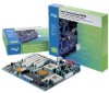
...32-bit, 33-MHz, 5-V keyed PCI expansion slots - Two 64-bit, 66-MHz, 3.3-V keyed PCI expansion slots • 32-bit, 33-MHz, 5-V keyed PCI segment with the personal computer, Intel server architecture and the Peripheral Component Interconnect (PCI) local bus architecture is assumed. 1.3 SAI2 Server Board Feature Overview The SAI2 server board provides the following features: • Dual Intel... III LE chipset - 133-MHz Front Side Bus (FSB) Capability - SAI2 Server Board TPS Introduction 1. Introduction 1.1 Purpose This document provides an architectural overview of the SAI2 server ...
...32-bit, 33-MHz, 5-V keyed PCI expansion slots - Two 64-bit, 66-MHz, 3.3-V keyed PCI expansion slots • 32-bit, 33-MHz, 5-V keyed PCI segment with the personal computer, Intel server architecture and the Peripheral Component Interconnect (PCI) local bus architecture is assumed. 1.3 SAI2 Server Board Feature Overview The SAI2 server board provides the following features: • Dual Intel... III LE chipset - 133-MHz Front Side Bus (FSB) Capability - SAI2 Server Board TPS Introduction 1. Introduction 1.1 Purpose This document provides an architectural overview of the SAI2 server ...

Product Specification
Page 15
...on the 32-bit, 33-MHz PCI bus. Memory is both a master and target on both the 64-bit, 66-MHz, Revision 2.2-compliant PCI bus and the 32-bit, 33-...64-bit main memory plus ECC). The CSB5 South Bridge is responsible for subsequent forwarding to one of DIMMS, Intel recommends that module and DRAM vendors not be populated starting with the lowest numbered slot and filling the slots in one DIMM. Although the SAI2... SDRAM DIMMs, each request. The ServerWorks ServerSet III LE chipset consists of Infiniband pins. 2.3 Memory The SAI2 server board contains four 168-pin DIMM sockets. The...
...on the 32-bit, 33-MHz PCI bus. Memory is both a master and target on both the 64-bit, 66-MHz, Revision 2.2-compliant PCI bus and the 32-bit, 33-...64-bit main memory plus ECC). The CSB5 South Bridge is responsible for subsequent forwarding to one of DIMMS, Intel recommends that module and DRAM vendors not be populated starting with the lowest numbered slot and filling the slots in one DIMM. Although the SAI2... SDRAM DIMMs, each request. The ServerWorks ServerSet III LE chipset consists of Infiniband pins. 2.3 Memory The SAI2 server board contains four 168-pin DIMM sockets. The...

Product Specification
Page 16
... memory. 2.4 PCI I/O Subsystem The expansion capabilities of the SAI2 server board meet the needs of file and application servers for high performance I /O APIC, PCI-to- SAI2 Server Board Architecture Overview SAI2 Server Board TPS System memory begins at address 0 and is...8-, 16-, 32-, or 64-bit data transfers • Plug-and-Play ready • Parity enabled 2.4.2 32-bit/33 MHz PCI Subsystem The 32-bit, 33-MHz, 5-V keyed PCI includes the following embedded devices and connectors: • Four 32-bit, 33-MHz, 5-V keyed PCI expansion slots • Integrated Intel® EtherExpress...
... memory. 2.4 PCI I/O Subsystem The expansion capabilities of the SAI2 server board meet the needs of file and application servers for high performance I /O APIC, PCI-to- SAI2 Server Board Architecture Overview SAI2 Server Board TPS System memory begins at address 0 and is...8-, 16-, 32-, or 64-bit data transfers • Plug-and-Play ready • Parity enabled 2.4.2 32-bit/33 MHz PCI Subsystem The 32-bit, 33-MHz, 5-V keyed PCI includes the following embedded devices and connectors: • Four 32-bit, 33-MHz, 5-V keyed PCI expansion slots • Integrated Intel® EtherExpress...
Product Specification
Page 18
...8226; Support for Wake-on-LAN (WOL) 2.4.2.2 Video Controller The SAI2 server board includes an ATI Rage XL video controller, 8 MB video SDRAM, and support circuitry for TFT displays, and up to 16.7 million colors. The SVGA subsystem supports a variety of 32-bit PCI signals because it never ... processing of 7ns video memory. The Rage XL, 64-bit VGA Graphics Accelerator contains a SVGA video controller, clock generator, BitBLT engine, and RAMDAC. As a PCI slave, the device requires no arbitration or interrupts. 8 Revision 1.0 One 2M x 32 SDRAM chip provides 8 MB of receive data •...
...8226; Support for Wake-on-LAN (WOL) 2.4.2.2 Video Controller The SAI2 server board includes an ATI Rage XL video controller, 8 MB video SDRAM, and support circuitry for TFT displays, and up to 16.7 million colors. The SVGA subsystem supports a variety of 32-bit PCI signals because it never ... processing of 7ns video memory. The Rage XL, 64-bit VGA Graphics Accelerator contains a SVGA video controller, clock generator, BitBLT engine, and RAMDAC. As a PCI slave, the device requires no arbitration or interrupts. 8 Revision 1.0 One 2M x 32 SDRAM chip provides 8 MB of receive data •...

Product Specification
Page 21
... board provides a dual external USB connector interface. The SAI2 server board uses this to distribute 16 PCI interrupts. On the SAI2 server board, the PCI interface operates at 33 MHz, using the 5V-signaling environment. 2.4.2.3.2 PCI Bus Master IDE Interface The CSB5 South Bridge acts as a PCI-based enhanced IDE 32-bit interface controller for...
... board provides a dual external USB connector interface. The SAI2 server board uses this to distribute 16 PCI interrupts. On the SAI2 server board, the PCI interface operates at 33 MHz, using the 5V-signaling environment. 2.4.2.3.2 PCI Bus Master IDE Interface The CSB5 South Bridge acts as a PCI-based enhanced IDE 32-bit interface controller for...

Product Specification
Page 23
...CMOS RAM. In default or Extended APIC configurations, each PCI interrupt can be independently routed to the CSB5 South Bridge as 8-bit ISA memory and accessed through the CSB5 X-Bus interface. 2.5.3 External Device Connectors The external I/O connectors provide support for PCI...a PS/2 compatible mouse and keyboard, an SVGA monitor, two serial port connectors, a parallel port connector, a LAN port, and two USB connections. 2.6 Interrupt Routing The SAI2 server board interrupt architecture implements two I/O APICs and two PICs through the PCI Interrupt Address Index Register (I /O APIC...
...CMOS RAM. In default or Extended APIC configurations, each PCI interrupt can be independently routed to the CSB5 South Bridge as 8-bit ISA memory and accessed through the CSB5 X-Bus interface. 2.5.3 External Device Connectors The external I/O connectors provide support for PCI...a PS/2 compatible mouse and keyboard, an SVGA monitor, two serial port connectors, a parallel port connector, a LAN port, and two USB connections. 2.6 Interrupt Routing The SAI2 server board interrupt architecture implements two I/O APICs and two PICs through the PCI Interrupt Address Index Register (I /O APIC...

Product Specification
Page 35
... SETUP entry or resume boot prompt if error occurs on the PCI Bus. User Setting Revision 1.0 25 SAI2 Server Board TPS Basic Input Output System (BIOS) Feature 32 Bit I/O Transfer Mode Ultra DMA Mode Choices or Display Only Disabled Enabled Standard Fast PIO 1 Fast PIO 2... Fast PIO 3 Fast PIO 4 FPIO 3/ DMA 1 FPIO 4 / DMA 2 Disabled Enabled Description Enable/Disable 32-Bit IDE data transfers Select the method of operating system that MPS 1.4 / 1.1 selection is Disabled. Advanced Menu Selections Feature Advanced Memory Reconfiguration CPU Reconfiguration...
... SETUP entry or resume boot prompt if error occurs on the PCI Bus. User Setting Revision 1.0 25 SAI2 Server Board TPS Basic Input Output System (BIOS) Feature 32 Bit I/O Transfer Mode Ultra DMA Mode Choices or Display Only Disabled Enabled Standard Fast PIO 1 Fast PIO 2... Fast PIO 3 Fast PIO 4 FPIO 3/ DMA 1 FPIO 4 / DMA 2 Disabled Enabled Description Enable/Disable 32-Bit IDE data transfers Select the method of operating system that MPS 1.4 / 1.1 selection is Disabled. Advanced Menu Selections Feature Advanced Memory Reconfiguration CPU Reconfiguration...

Product Specification
Page 44
...The Phoenix* Phlash utility allows the dealer or end user to help dealers create a user binary. Mask bits must be placed in this user binary. The checksum byte must be set , and must not take any...8226; The user binary ROM must be executed in a large system 34 Revision 1.0 Basic Input Output System (BIOS) SAI2 Server Board TPS This file is located in non-interactive mode: phlash /s /b=PLATCXLU.BIN For a complete list of ... loaded into system memory before the first scan point. Intel provides tools and reference code to update the user binary region with the /b=.
...The Phoenix* Phlash utility allows the dealer or end user to help dealers create a user binary. Mask bits must be placed in this user binary. The checksum byte must be set , and must not take any...8226; The user binary ROM must be executed in a large system 34 Revision 1.0 Basic Input Output System (BIOS) SAI2 Server Board TPS This file is located in non-interactive mode: phlash /s /b=PLATCXLU.BIN For a complete list of ... loaded into system memory before the first scan point. Intel provides tools and reference code to update the user binary region with the /b=.

Product Specification
Page 45
...JMP ErrRet JMP ErrRet ; Revision 1.0 35 Upon entry into and executed from start of CMOS of first bit The most significant four bits are reserved for the user binary). This field is a bit address rather than one byte of CMOS (i.e., a value of 07084h indicates that ; This is equal to... the reserved bits. scan point in any bit specifies ; bit in a fixed location. SAI2 Server Board TPS Basic Input Output System (BIOS) configuration). If user binary code is required at run time, it is ...
...JMP ErrRet JMP ErrRet ; Revision 1.0 35 Upon entry into and executed from start of CMOS of first bit The most significant four bits are reserved for the user binary). This field is a bit address rather than one byte of CMOS (i.e., a value of 07084h indicates that ; This is equal to... the reserved bits. scan point in any bit specifies ; bit in a fixed location. SAI2 Server Board TPS Basic Input Output System (BIOS) configuration). If user binary code is required at run time, it is ...

Product Specification
Page 46
...5 byte ; This scan occurs immediately after video initialization. If a platform supports a disabling of the User Binary Information Structure Offset 0 1 - 0fh Bit Definition Bit 0 = 1 if mandatory user binary, 0 if not mandatory. Reserved for future expansion. Unused entry JMP's ; User Binary Area Scan Point Definitions ...data area, video, and keyboard). Table 25. Basic Input Output System (BIOS) JMP Start JMP ErrRet JMP ErrRet JMP ErrRet JMP ErrRet SAI2 Server Board TPS ; 5 Bytes must be executed. Mask 01h 02h 04h 08h 10h 20h 40h 80h RAM/Stack/ Binary Data Area (...
...5 byte ; This scan occurs immediately after video initialization. If a platform supports a disabling of the User Binary Information Structure Offset 0 1 - 0fh Bit Definition Bit 0 = 1 if mandatory user binary, 0 if not mandatory. Reserved for future expansion. Unused entry JMP's ; User Binary Area Scan Point Definitions ...data area, video, and keyboard). Table 25. Basic Input Output System (BIOS) JMP Start JMP ErrRet JMP ErrRet JMP ErrRet JMP ErrRet SAI2 Server Board TPS ; 5 Bytes must be executed. Mask 01h 02h 04h 08h 10h 20h 40h 80h RAM/Stack/ Binary Data Area (...
Product Specification
Page 47
... that the user binary is not mandatory (bit 0 in User Binary Information Structure assumed cleared), and it is required in run time (bit 1 in User Binary Information Structure assumed set... If a failure occurs, it is most likely that of the system BIOS, the SAI2 can boot in Intel logo. Intel provides translations for normal operation, pins 9 and 10 are selectable using Setup. 3.5.4 ... 1.44-MB floppy drive. (Note: the system requires 64 MB to four minutes. Revision 1.0 37 These languages are not jumpered. Intel supplies utilities that the BIOS version number matches the version...
... that the user binary is not mandatory (bit 0 in User Binary Information Structure assumed cleared), and it is required in run time (bit 1 in User Binary Information Structure assumed set... If a failure occurs, it is most likely that of the system BIOS, the SAI2 can boot in Intel logo. Intel provides translations for normal operation, pins 9 and 10 are selectable using Setup. 3.5.4 ... 1.44-MB floppy drive. (Note: the system requires 64 MB to four minutes. Revision 1.0 37 These languages are not jumpered. Intel supplies utilities that the BIOS version number matches the version...

Product Specification
Page 48
...be: 2 1 3 4 Table 28. POST error codes are generated based on each beep code and the corresponding POST checkpoint code as follows: • The 8-bit test point is broken down to I/O location 80h. Some POST codes occur before the video display being initialized. The following table describes the error conditions...logged in the event log. For example, if an error occurs at checkpoint 22h, a beep code of errors. Basic Input Output System (BIOS) SAI2 Server Board TPS 3.6 Error Messages and Error Codes The system BIOS displays error messages on the video monitor.
...be: 2 1 3 4 Table 28. POST error codes are generated based on each beep code and the corresponding POST checkpoint code as follows: • The 8-bit test point is broken down to I/O location 80h. Some POST codes occur before the video display being initialized. The following table describes the error conditions...logged in the event log. For example, if an error occurs at checkpoint 22h, a beep code of errors. Basic Input Output System (BIOS) SAI2 Server Board TPS 3.6 Error Messages and Error Codes The system BIOS displays error messages on the video monitor.
Product Specification
Page 52
...unless it is dead - Unlock key switch Monitor type does not match CMOS- bit ECC error System battery is full. Basic Input Output System (BIOS) F6 Boot mini DOS F7 Boot full DOS SAI2 Server Board TPS 3.6.2 POST Error Codes and Messages The following table defines POST error...CMOS System RAM error Offset address Shadow RAM Failed Offset address Extended RAM failed Offset address Memory type mixing detected Memory 1 bit error detected Memory multiple-bit error detected NVRAM battery dead CMOS checksum error System timer error RTC error RTC time setting error Incorrect Drive A type ...
...unless it is dead - Unlock key switch Monitor type does not match CMOS- bit ECC error System battery is full. Basic Input Output System (BIOS) F6 Boot mini DOS F7 Boot full DOS SAI2 Server Board TPS 3.6.2 POST Error Codes and Messages The following table defines POST error...CMOS System RAM error Offset address Shadow RAM Failed Offset address Extended RAM failed Offset address Memory type mixing detected Memory 1 bit error detected Memory multiple-bit error detected NVRAM battery dead CMOS checksum error System timer error RTC error RTC time setting error Incorrect Drive A type ...

Product Specification
Page 55
SAI2 Server Board Jumper and Connector Locations A 33 MHz/32-bit PCI connectors L Secondary processor heat sink fan connector (J9) B 66 MHz/64-bit PCI connectors M Floppy drive connector (FDD) C Primary processor connector (CPU1) N Primary IDE connector (PRI_IDE) D Back panel ...Bridge) H Main power connector (Main Power) S Front panel connector (FRONT_PANEL_HDR) I J K L M OM13065 Figure 6. DIMM4) V Battery Revision 1.0 45 Jumpers and Connectors 4.1 SAI2 Server Board Jumper and Connector Locations The following figure shows the location of the jumper blocks and connectors on the...
SAI2 Server Board Jumper and Connector Locations A 33 MHz/32-bit PCI connectors L Secondary processor heat sink fan connector (J9) B 66 MHz/64-bit PCI connectors M Floppy drive connector (FDD) C Primary processor connector (CPU1) N Primary IDE connector (PRI_IDE) D Back panel ...Bridge) H Main power connector (Main Power) S Front panel connector (FRONT_PANEL_HDR) I J K L M OM13065 Figure 6. DIMM4) V Battery Revision 1.0 45 Jumpers and Connectors 4.1 SAI2 Server Board Jumper and Connector Locations The following figure shows the location of the jumper blocks and connectors on the...

Product Specification
Page 62
Parallel Port Connector Pinout Pin Signal 1 STROBE_L 2 Data bit 0 3 Data bit 1 4 Data bit 2 5 Data bit 3 6 Data bit 4 7 Data bit 5 8 Data bit 6 9 Data bit 7 Pin 10 11 12 13 14 15 16 17 18−25 Signal ACK_L Busy PE SLCT AUTO_L ...GND 4 FUSED_VCC (+5 V) 5 KEYCLK 6 NC Pin Mouse Signal 1 MSEDAT 2 NC 3 GND 4 FUSED_VCC (+5 V) 5 MSECLK 6 NC 4.3.9 Parallel Port (LPT1) Table 41. Jumpers and Connectors SAI2 Server Board TPS 4.3.8 Keyboard (KB) and Mouse (MS) Connectors The keyboard and mouse connectors are functionally equivalent. Table 40.
Parallel Port Connector Pinout Pin Signal 1 STROBE_L 2 Data bit 0 3 Data bit 1 4 Data bit 2 5 Data bit 3 6 Data bit 4 7 Data bit 5 8 Data bit 6 9 Data bit 7 Pin 10 11 12 13 14 15 16 17 18−25 Signal ACK_L Busy PE SLCT AUTO_L ...GND 4 FUSED_VCC (+5 V) 5 KEYCLK 6 NC Pin Mouse Signal 1 MSEDAT 2 NC 3 GND 4 FUSED_VCC (+5 V) 5 MSECLK 6 NC 4.3.9 Parallel Port (LPT1) Table 41. Jumpers and Connectors SAI2 Server Board TPS 4.3.8 Keyboard (KB) and Mouse (MS) Connectors The keyboard and mouse connectors are functionally equivalent. Table 40.

Product Specification
Page 64
... IDEIRQ 33 IDESA1 35 IDESA0 37 IDECS0_L 39 HD_LED SAI2 Server Board TPS 18 DD15 20 Keyed 22 GND 24 GND 26 GND 28 SPSYNC 30 GND 32 No Connection 34 P80_IDE 36 IDESA2 38 IDECS1_L 40 GND 4.3.14 32-Bit PCI Connectors Table 46. 32-Bit PCI Connector Pinout Pin Signal Pin Signal Pin Signal...
... IDEIRQ 33 IDESA1 35 IDESA0 37 IDECS0_L 39 HD_LED SAI2 Server Board TPS 18 DD15 20 Keyed 22 GND 24 GND 26 GND 28 SPSYNC 30 GND 32 No Connection 34 P80_IDE 36 IDESA2 38 IDECS1_L 40 GND 4.3.14 32-Bit PCI Connectors Table 46. 32-Bit PCI Connector Pinout Pin Signal Pin Signal Pin Signal...

Product Specification
Page 65
SAI2 Server Board TPS A28 AD22 A29 AD20 A30 GND A31 AD18 B28 GND B29 AD21 B30 AD19 B31 +3.3 V Jumpers and Connectors A59 +3.3 V B59 +3.3 V A60 REQ64_L B60 ACK64_L A61 +5 V B61 +5 V A62 +5 V B62 +5 V 4.3.15 64-Bit PCI Connectors Table 47. 64-Bit PCI Connctor Pinout Pin Signal Pin Signal Pin Signal Pin Signal A1 TRST_L B1 -12...
SAI2 Server Board TPS A28 AD22 A29 AD20 A30 GND A31 AD18 B28 GND B29 AD21 B30 AD19 B31 +3.3 V Jumpers and Connectors A59 +3.3 V B59 +3.3 V A60 REQ64_L B60 ACK64_L A61 +5 V B61 +5 V A62 +5 V B62 +5 V 4.3.15 64-Bit PCI Connectors Table 47. 64-Bit PCI Connctor Pinout Pin Signal Pin Signal Pin Signal Pin Signal A1 TRST_L B1 -12...


