Specifications
Page 1
K6602637 Rev.3 02.27.01 H I T A C H I All Rights Reserved, Copyright ©2001 Hitachi, Ltd. (Total 104 pages) - 1 - OEM Manual DK23CA-30F/30/15/75 Disk Drive Specifications REV.3 Caution for Safety Read Safety descriptions carefully. Keep this manual with care. Read and recommend drive usage cautions to your end user.
K6602637 Rev.3 02.27.01 H I T A C H I All Rights Reserved, Copyright ©2001 Hitachi, Ltd. (Total 104 pages) - 1 - OEM Manual DK23CA-30F/30/15/75 Disk Drive Specifications REV.3 Caution for Safety Read Safety descriptions carefully. Keep this manual with care. Read and recommend drive usage cautions to your end user.

Specifications
Page 2
...Items of this product. (Caution before attempting to insure unlimited use. Handling Page 4 Sec. 1.2, Page 10 - 11 Sec.3.1, Page 14 Sec. 3.2, Page 15 Sec. 3.2, Page 16 Sec. 4.2.3, Page 21 Sec. 5.1, Page 23 Sec. 5.2, Page 24 -...injury or damage to follow the instructions on "Safety Instructions" (Page 4) and "1.2 General Caution" (Page 10 and 11) before Product Use) - Safety Instructions - l Advise your end users read safety descriptions below ...01 Preliminary Rev.1: 02.08.01 Preliminary Rev.2: 02:15:01 Rev.3: 02:27:01 To use this product safely To use the product, read the ...
...Items of this product. (Caution before attempting to insure unlimited use. Handling Page 4 Sec. 1.2, Page 10 - 11 Sec.3.1, Page 14 Sec. 3.2, Page 15 Sec. 3.2, Page 16 Sec. 4.2.3, Page 21 Sec. 5.1, Page 23 Sec. 5.2, Page 24 -...injury or damage to follow the instructions on "Safety Instructions" (Page 4) and "1.2 General Caution" (Page 10 and 11) before Product Use) - Safety Instructions - l Advise your end users read safety descriptions below ...01 Preliminary Rev.1: 02.08.01 Preliminary Rev.2: 02:15:01 Rev.3: 02:27:01 To use this product safely To use the product, read the ...

Specifications
Page 3
...product, such as EMC standard EN55022 (corresponding to FCC part 15 Class B, etc.). IEC60950 A4: 1996 - In general, Hitachi shall not be responsible for products which have been changed by anyone else. HITACHIɹSHALL NOT BE LIABLE FOR ANY SPECIAL, INCIDENTAL OR ...However, anything other products or equipment. Therefore, the following safety regulations, but the system side should change this product Hitachi assumes no event will Hitachi be further limited in the event the product fails to conform to the original purchaser in accordance with its sales ...
...product, such as EMC standard EN55022 (corresponding to FCC part 15 Class B, etc.). IEC60950 A4: 1996 - In general, Hitachi shall not be responsible for products which have been changed by anyone else. HITACHIɹSHALL NOT BE LIABLE FOR ANY SPECIAL, INCIDENTAL OR ...However, anything other products or equipment. Therefore, the following safety regulations, but the system side should change this product Hitachi assumes no event will Hitachi be further limited in the event the product fails to conform to the original purchaser in accordance with its sales ...
Specifications
Page 4
... damage to circuit or component failure. Label or seal shall be under below GND level (0 V) at power on PCBA), it may occur. 15. Contact causes pin dent, electrical discharge distraction or contact failure. Also, pins or HDA corners may contact to the PCBA of opened HDA or ..., etc.) adheres to the connector insertion or jumper setting can damage the drive. on is often incurred by the system. Customer should be swapped during handling. 10. Shock can result in permanent damage to the drive and/or loss of screws and the torque recommended in life support devices or...
... damage to circuit or component failure. Label or seal shall be under below GND level (0 V) at power on PCBA), it may occur. 15. Contact causes pin dent, electrical discharge distraction or contact failure. Also, pins or HDA corners may contact to the PCBA of opened HDA or ..., etc.) adheres to the connector insertion or jumper setting can damage the drive. on is often incurred by the system. Customer should be swapped during handling. 10. Shock can result in permanent damage to the drive and/or loss of screws and the torque recommended in life support devices or...
Specifications
Page 6
... 2 9 9 10 12 13 13 15 16 17 17 17...DRIVE 0/DRIVE 1) 4.4 Dimensions 5.0 Packing and Handling 5.1 Packing 5.2 Handling 6.0 Interface 6.1 Power Interface 6.2 Physical Interface 6.2.1 Connector 6.2.2 Connector Pin Assignment 6.2.3 Description of the Interface Signals 6.3 Logical Interface 6.3.1 I/O Registers 6.3.1.1 Data Register 6.3.1.2 Error Register 6.3.1.3 Features Register 6.3.1.4 Sector Count Register 6.3.1.5 Sector Number Register 6.3.1.6 Cylinder Low Register 6.3.1.7 Cylinder High Register 6.3.1.8 Device/Head Register 6.3.1.9 Status Register 6.3.1.10...
... 2 9 9 10 12 13 13 15 16 17 17 17...DRIVE 0/DRIVE 1) 4.4 Dimensions 5.0 Packing and Handling 5.1 Packing 5.2 Handling 6.0 Interface 6.1 Power Interface 6.2 Physical Interface 6.2.1 Connector 6.2.2 Connector Pin Assignment 6.2.3 Description of the Interface Signals 6.3 Logical Interface 6.3.1 I/O Registers 6.3.1.1 Data Register 6.3.1.2 Error Register 6.3.1.3 Features Register 6.3.1.4 Sector Count Register 6.3.1.5 Sector Number Register 6.3.1.6 Cylinder Low Register 6.3.1.7 Cylinder High Register 6.3.1.8 Device/Head Register 6.3.1.9 Status Register 6.3.1.10...
Specifications
Page 9
... latest high-density recording technology. Low Power Consumption: 0.65W(130mA) at Idle mode, 0.25W(50mA) at Standby mode - 1.0 General 1.1 Introduction The DK23CA series disk drives reach high capacities (30,005MB, 15,103MB and 7,501MB for Setup] Table 1.1 Identify Device information (Addressing) Model Word 1 Word 3 Word 6 Word 60Ŋ61 Number of SPT Total...
... latest high-density recording technology. Low Power Consumption: 0.65W(130mA) at Idle mode, 0.25W(50mA) at Standby mode - 1.0 General 1.1 Introduction The DK23CA series disk drives reach high capacities (30,005MB, 15,103MB and 7,501MB for Setup] Table 1.1 Identify Device information (Addressing) Model Word 1 Word 3 Word 6 Word 60Ŋ61 Number of SPT Total...
Specifications
Page 12
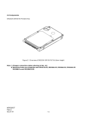
2.0 Components DK23CA-30F/30/15/75 Disk Drive Figure 2-1 Overview of DK23CA-30F/30/15/75 (9.5mm height) Note: 1) Prepare connection cables referring to Sec. 6.2. 2) Mounting holes are compatible with DK237A-XX, DK238A-XX, DK239A-XX, DK23AA-XX DK23BA-xx and DK23BA-XXE. K6602637 Rev.3 02.27.01 - 12 -
2.0 Components DK23CA-30F/30/15/75 Disk Drive Figure 2-1 Overview of DK23CA-30F/30/15/75 (9.5mm height) Note: 1) Prepare connection cables referring to Sec. 6.2. 2) Mounting holes are compatible with DK237A-XX, DK238A-XX, DK239A-XX, DK23AA-XX DK23BA-xx and DK23BA-XXE. K6602637 Rev.3 02.27.01 - 12 -
Specifications
Page 13
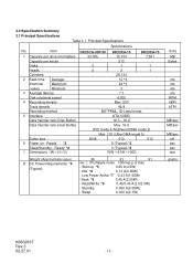
... A(1.65W) -Seek *8 0.45 A(2.25W) - Read/Write *9 0.40/0.40 A(2.0/2.0W) - Standby 0.050 A(0.25W) - Item 1 Capacity per drive (Formatted) Capacity per sector Disks Heads Cylinders 2 Seek time Average (Nominal Maximum value) Minimum 3 Average latency Disk rotational speed 4 Recording density Track ...transfer rate (Disk-Buffer) Data transfer rate (Host-Buffer) Buffer size 6 Power on - Ready *2 7 DimensionsʢWʷHʷD) DK23CA-30F/30 DK23CA-15 DK23CA-75 30,005 15,103 7,501 512 2 1 1 4 2 1 28,134 12 *1 24 *1 3 7.1 4,200 Max. 530 46.8 ME2PRML,...
... A(1.65W) -Seek *8 0.45 A(2.25W) - Read/Write *9 0.40/0.40 A(2.0/2.0W) - Standby 0.050 A(0.25W) - Item 1 Capacity per drive (Formatted) Capacity per sector Disks Heads Cylinders 2 Seek time Average (Nominal Maximum value) Minimum 3 Average latency Disk rotational speed 4 Recording density Track ...transfer rate (Disk-Buffer) Data transfer rate (Host-Buffer) Buffer size 6 Power on - Ready *2 7 DimensionsʢWʷHʷD) DK23CA-30F/30 DK23CA-15 DK23CA-75 30,005 15,103 7,501 512 2 1 1 4 2 1 28,134 12 *1 24 *1 3 7.1 4,200 Max. 530 46.8 ME2PRML,...
Specifications
Page 15
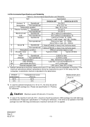
... months. *3 : In case of the maximum wet bulb 40°C , the drive should be measured at point 10 mm away from the nameplate, a substitution method is applied. 3.2 Environmental Specifications and Reliability Table 3.2 Environmental Specification and Reliability No. Item Specification DK23CA-30F DK23CA-30/15/75 1 Ambient *1 Operational 5 to 55°C temperature Non-operational -40 to...
... months. *3 : In case of the maximum wet bulb 40°C , the drive should be measured at point 10 mm away from the nameplate, a substitution method is applied. 3.2 Environmental Specifications and Reliability Table 3.2 Environmental Specification and Reliability No. Item Specification DK23CA-30F DK23CA-30/15/75 1 Ambient *1 Operational 5 to 55°C temperature Non-operational -40 to...
Specifications
Page 18
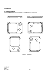
K6602637 Rev.3 02.27.01 Figure 4-1 Installation - 18 - 4.0 Installation 4.1 Installation Direction The DK23CA-30F/30/15/75 can be installed in the 6 directions as shown below.
K6602637 Rev.3 02.27.01 Figure 4-1 Installation - 18 - 4.0 Installation 4.1 Installation Direction The DK23CA-30F/30/15/75 can be installed in the 6 directions as shown below.
Specifications
Page 22
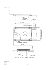
full thread 76.6 ± 0.25 14.0 ± 0.25 10.24 ± 0.25 61.72±0.25 4-M3 3.0mm min. full thread 100±0.45 3.99ʶ0.25 K6602637 Rev.3 02.27.01 2 42 (Unit : mm) Figure 4-4 Dimensions (DK23CA-30F/30/15/75) - 22 - 3ʶ0.25 4.07±0.25 10.14±0.375 69.85ʶ0.25 Drive width at mounting (70.1 Maximum drive width) 9.5 ʶ 0.2 2 4.4 Dimensions 4-M3 3.5mm min.
full thread 76.6 ± 0.25 14.0 ± 0.25 10.24 ± 0.25 61.72±0.25 4-M3 3.0mm min. full thread 100±0.45 3.99ʶ0.25 K6602637 Rev.3 02.27.01 2 42 (Unit : mm) Figure 4-4 Dimensions (DK23CA-30F/30/15/75) - 22 - 3ʶ0.25 4.07±0.25 10.14±0.375 69.85ʶ0.25 Drive width at mounting (70.1 Maximum drive width) 9.5 ʶ 0.2 2 4.4 Dimensions 4-M3 3.5mm min.
Specifications
Page 27
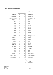
çç6.2.2 Connector Pin Assignment Figure 6-4 Pin Assignments JUMPER1 A JUMPER3 C KEY(Removed) E RESET- 1 DD7 3 DD6 5 DD5 7 DD4 9 DD3 11 DD2 13 DD1 15 DD0 17 GND 19 DMARQ 21 DIOW- 23 DIOR- 25 IORDY 27 DMACK- 29 INTRQ 31 DA1 33 DA0 35 CS0- 37 DASP- 39 5VDC(...Logic) 41 GND(Logic) 43 B JUMPER0 D JUMPER2 F KEY(Removed) 2 GND 4 DD8 6 DD9 8 DD10 10 DD11 12 DD12 14 DD13 16 DD14 18 DD15 20 KEY(Removed) 22 GND 24 GND 26 GND 28 CSEL 30 GND 32 IOCS16- 34...
çç6.2.2 Connector Pin Assignment Figure 6-4 Pin Assignments JUMPER1 A JUMPER3 C KEY(Removed) E RESET- 1 DD7 3 DD6 5 DD5 7 DD4 9 DD3 11 DD2 13 DD1 15 DD0 17 GND 19 DMARQ 21 DIOW- 23 DIOR- 25 IORDY 27 DMACK- 29 INTRQ 31 DA1 33 DA0 35 CS0- 37 DASP- 39 5VDC(...Logic) 41 GND(Logic) 43 B JUMPER0 D JUMPER2 F KEY(Removed) 2 GND 4 DD8 6 DD9 8 DD10 10 DD11 12 DD12 14 DD13 16 DD14 18 DD15 20 KEY(Removed) 22 GND 24 GND 26 GND 28 CSEL 30 GND 32 IOCS16- 34...

Specifications
Page 28
Reserved pins should be used to configure a device as either DRIVE 0 or DRIVE1 when CSEL mode is pulled up inside the drive. "I" of the Ultra DMA burst. This signal is a reset signal output from the device. This signal is selected. Table 6.2 shows signal definitions. ... of the Interface Signals The interface is ready to receive Ultra DMA Write data . Both the rising and falling edge latch the data from DD(15:0) into the device. I /O This is ready to receive Ultra DMA Read data . I Activating this Read Strobe signal enables data from the device ...
Reserved pins should be used to configure a device as either DRIVE 0 or DRIVE1 when CSEL mode is pulled up inside the drive. "I" of the Ultra DMA burst. This signal is a reset signal output from the device. This signal is selected. Table 6.2 shows signal definitions. ... of the Interface Signals The interface is ready to receive Ultra DMA Write data . Both the rising and falling edge latch the data from DD(15:0) into the device. I /O This is ready to receive Ultra DMA Read data . I Activating this Read Strobe signal enables data from the device ...

Specifications
Page 32
... executed successfully. Not Ready and Write fault) or an invalid command code. When a command has been completed and the value of this register contains Bits 15-8 of the LBA. 6.3.1.7 Cylinder High Register This register contains the higher 8 bits of the starting cylinder address for any disk data access. This definition cannot...
... executed successfully. Not Ready and Write fault) or an invalid command code. When a command has been completed and the value of this register contains Bits 15-8 of the LBA. 6.3.1.7 Cylinder High Register This register contains the higher 8 bits of the starting cylinder address for any disk data access. This definition cannot...
Specifications
Page 38
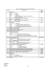
... supported Bit 8 1 = DMA supported Bit 7 - 0 Vendor Specific Value (HEX.) 045Ah See table 6.6 C837h See table 6.6 See table 6.6 0003h DK23CA-15/ 75: 0400h DK23CA-30F/ 30: 1000h 0004h 8010h 0000h 0B00h K6602637 Rev.3 02.27.01 - 38 - The host then reads the information from the device. When the... 4 Number of unformatted bytes per track 5 Number of unformatted bytes per sector 6 Number of logical sectors per logical track 7-9 Vendor specific 10-19 Serial number (20 ASCII characters) 20 Buffer type 0000h = Not specified 0001h = Single port single buffer 0002h = Dual port multi-...
... supported Bit 8 1 = DMA supported Bit 7 - 0 Vendor Specific Value (HEX.) 045Ah See table 6.6 C837h See table 6.6 See table 6.6 0003h DK23CA-15/ 75: 0400h DK23CA-30F/ 30: 1000h 0004h 8010h 0000h 0B00h K6602637 Rev.3 02.27.01 - 38 - The host then reads the information from the device. When the... 4 Number of unformatted bytes per track 5 Number of unformatted bytes per sector 6 Number of logical sectors per logical track 7-9 Vendor specific 10-19 Serial number (20 ASCII characters) 20 Buffer type 0000h = Not specified 0001h = Single port single buffer 0002h = Dual port multi-...
Specifications
Page 39
... DMA Cycle Time(ns) Minimum PIO Transfer Cycle Time without Flow Control(ns) Minimum PIO Transfer Cycle Time with IORDY(ns) Reserved Queue Depth Bit 15 - 5 0 = Reserved Bit 4 - 0 Maximum queue depth Reserved Value (HEX.) 4000h 0200h 0200h 0007h See table 6.6 0003h 0078h 0078h 0190h 0078h 0000h 0000h 0000h K6602637 Rev.3 02... 51 52 53 54 55 56 57-58 59 60-61 62 63 64 65 66 67 68 69-74 75 76-79 Capabilities Bit 15 0 (fixed) Bit 14 1 (fixed) Bit 13 - 1 0 = Reserved Bit 0 1 = Standby timer value is valid Bit 7 - 0Current setting for number of sectors that can be transferred per...
... DMA Cycle Time(ns) Minimum PIO Transfer Cycle Time without Flow Control(ns) Minimum PIO Transfer Cycle Time with IORDY(ns) Reserved Queue Depth Bit 15 - 5 0 = Reserved Bit 4 - 0 Maximum queue depth Reserved Value (HEX.) 4000h 0200h 0200h 0007h See table 6.6 0003h 0078h 0078h 0190h 0078h 0000h 0000h 0000h K6602637 Rev.3 02... 51 52 53 54 55 56 57-58 59 60-61 62 63 64 65 66 67 68 69-74 75 76-79 Capabilities Bit 15 0 (fixed) Bit 14 1 (fixed) Bit 13 - 1 0 = Reserved Bit 0 1 = Standby timer value is valid Bit 7 - 0Current setting for number of sectors that can be transferred per...
Specifications
Page 40
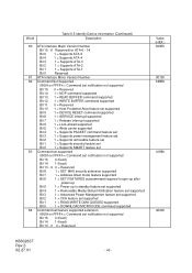
... 14 1 = NOP command supported Bit 13 1 = READ BUFFER command supported Bit 12 1 = WRITE BUFFER command supported Bit 11 0 = Reserved Bit 10 1 = Host Protected Area feature set supported Bit 9 1 = DEVICE RESET command supported Bit 8 1 = SERVICE interrupt supported Bit 7 1 = Release interrupt... Bit 1 1 = Supports security feature set Bit 0 1 = Supports SMART feature set 83 Command set supported 0000h or FFFFh = Command set notification not supported Bit 15 0 (fixed) Bit 14 1 (fixed) Bit 13 - 9 0 = Reserved Bit 8 1 = SET MAX security extension supported Bit 7 1 = Address offset...
... 14 1 = NOP command supported Bit 13 1 = READ BUFFER command supported Bit 12 1 = WRITE BUFFER command supported Bit 11 0 = Reserved Bit 10 1 = Host Protected Area feature set supported Bit 9 1 = DEVICE RESET command supported Bit 8 1 = SERVICE interrupt supported Bit 7 1 = Release interrupt... Bit 1 1 = Supports security feature set Bit 0 1 = Supports SMART feature set 83 Command set supported 0000h or FFFFh = Command set notification not supported Bit 15 0 (fixed) Bit 14 1 (fixed) Bit 13 - 9 0 = Reserved Bit 8 1 = SET MAX security extension supported Bit 7 1 = Address offset...
Specifications
Page 41
... 14 1 = NOP command supported Bit 13 1 = READ BUFFER command supported Bit 12 1 = WRITE BUFFER command supported Bit 11 0 = Reserved Bit 10 1 = Host Protected Area feature set supported Bit 9 1 = DEVICE RESET command supported Bit 8 1 = SERVICE interrupt enabled Bit 7 1 = Release ... 1 = READ/WRITE DMA QUEUED supported Bit 0 1 = DOWNLOAD MICROCODE command supported 87 Command set/feature default 0000h or FFFFh = Command set notification not supported Bit 15 0 (fixed) Bit 14 1 (fixed) Bit 13 - 0 0 = Reserved Value (HEX.) 3468h (at shipment) 0008h 4000h K6602637 Rev.3 02.27.01 -...
... 14 1 = NOP command supported Bit 13 1 = READ BUFFER command supported Bit 12 1 = WRITE BUFFER command supported Bit 11 0 = Reserved Bit 10 1 = Host Protected Area feature set supported Bit 9 1 = DEVICE RESET command supported Bit 8 1 = SERVICE interrupt enabled Bit 7 1 = Release ... 1 = READ/WRITE DMA QUEUED supported Bit 0 1 = DOWNLOAD MICROCODE command supported 87 Command set/feature default 0000h or FFFFh = Command set notification not supported Bit 15 0 (fixed) Bit 14 1 (fixed) Bit 13 - 0 0 = Reserved Value (HEX.) 3468h (at shipment) 0008h 4000h K6602637 Rev.3 02.27.01 -...

Specifications
Page 42
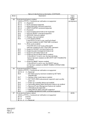
...Value (HEX.) XX3Fh 00XXh 00XXh 40XXh XXXXh K6602637 Rev.3 02.27.01 - 42 - Word Table 6.5 Identify Device Information (Continued) Description 88 Ultra DMA transfer Bit 15 - 14 0 = Reserved Bit 13 0 = Ultra DMA mode 5 is selected Bit 12 0 = Ultra DMA mode 4 is selected Bit 11 0 = Ultra DMA ...mode 3 is selected Bit 10 0 = Ultra DMA mode 2 is selected Bit 9 0 = Ultra DMA mode 1 is selected Bit 8 0 = Ultra DMA mode 0 is selected Bit 7 - 6 0 = Reserved Bit 5 0 = ...
...Value (HEX.) XX3Fh 00XXh 00XXh 40XXh XXXXh K6602637 Rev.3 02.27.01 - 42 - Word Table 6.5 Identify Device Information (Continued) Description 88 Ultra DMA transfer Bit 15 - 14 0 = Reserved Bit 13 0 = Ultra DMA mode 5 is selected Bit 12 0 = Ultra DMA mode 4 is selected Bit 11 0 = Ultra DMA ...mode 3 is selected Bit 10 0 = Ultra DMA mode 2 is selected Bit 9 0 = Ultra DMA mode 1 is selected Bit 8 0 = Ultra DMA mode 0 is selected Bit 7 - 6 0 = Reserved Bit 5 0 = ...

Specifications
Page 43
... = Device 0 passed diagnostic Bit 2 - 1 These bits indicate how Device 0 determined the device number: 00, 11 = Reserved 01 = A jumper was used 10 = the CSEL signal was used Bit 0 1 (fixed) 94-126 Reserved Value (HEX.) XXXXh 0000h K6602637 Rev.3 02.27.01 - 43 - above ViH 0 ...zero. Word Table 6.5 Identify Device Information (Continued) Description 93 Hardware reset result Bit 15 0 (fixed) Bit 14 1 (fixed) Bit 13 Bit 12 - 8 1 = Device detected CBLID- below ViL Device 1 hardware reset result. Bit 10 - 9 These bits indicate how Device 1 determined the device number: 00, 11 =...
... = Device 0 passed diagnostic Bit 2 - 1 These bits indicate how Device 0 determined the device number: 00, 11 = Reserved 01 = A jumper was used 10 = the CSEL signal was used Bit 0 1 (fixed) 94-126 Reserved Value (HEX.) XXXXh 0000h K6602637 Rev.3 02.27.01 - 43 - above ViH 0 ...zero. Word Table 6.5 Identify Device Information (Continued) Description 93 Hardware reset result Bit 15 0 (fixed) Bit 14 1 (fixed) Bit 13 Bit 12 - 8 1 = Device detected CBLID- below ViL Device 1 hardware reset result. Bit 10 - 9 These bits indicate how Device 1 determined the device number: 00, 11 =...