
User Guide
Page 14
... Identification Register 259 Supported TAP Instructions 259 Tag versus Data Selector 266 DR7 LEN and RW Definitions 273 Operating Ranges for Low-Power AMD-K6™-2E+ Devices . . 286 Operating Ranges for Standard-Power AMD-K6™-2E+ Devices 286 Absolute Ratings 287 DC Characteristics for the AMD-K6™-2E+ Processor 287 Power Dissipation for Low-Power AMD-K6™-2E...
... Identification Register 259 Supported TAP Instructions 259 Tag versus Data Selector 266 DR7 LEN and RW Definitions 273 Operating Ranges for Low-Power AMD-K6™-2E+ Devices . . 286 Operating Ranges for Standard-Power AMD-K6™-2E+ Devices 286 Absolute Ratings 287 DC Characteristics for the AMD-K6™-2E+ Processor 287 Power Dissipation for Low-Power AMD-K6™-2E...

User Guide
Page 23
... cache • Internal split, two-way set associative, 128-Kbyte, L2 Cache x Multiport internal cache design enabling simultaneous 64-bit reads/writes of L1 and L2 caches s Super7 platform is Socket 7-compatible x Leverages high-speed 100-MHz processor bus x 2x Accelerated Graphic Port (AGP) support Chapter 1 AMD-K6™-2E+ Embedded Processor 1 23542A/0-September 2000 Preliminary Information AMD-K6™-2E+ Embedded Processor Data Sheet 1 AMD-K6™-2E+ Embedded Processor...
... cache • Internal split, two-way set associative, 128-Kbyte, L2 Cache x Multiport internal cache design enabling simultaneous 64-bit reads/writes of L1 and L2 caches s Super7 platform is Socket 7-compatible x Leverages high-speed 100-MHz processor bus x 2x Accelerated Graphic Port (AGP) support Chapter 1 AMD-K6™-2E+ Embedded Processor 1 23542A/0-September 2000 Preliminary Information AMD-K6™-2E+ Embedded Processor Data Sheet 1 AMD-K6™-2E+ Embedded Processor...

User Guide
Page 24
... compute-intensive operations x Offers fast frame rates on demand while dissipating the lowest amount of power possible s 3DNow!™ technology for full 3.3 V I/O x Lower core voltages enable low-power operation s Operating frequencies x Standard-power and standard-temperature devices: 400, 450, and 500 MHz x Low-power and extended-temperature devices: 350, 400, and 450 MHz 2 AMD-K6™-2E+ Embedded Processor Chapter 1
... compute-intensive operations x Offers fast frame rates on demand while dissipating the lowest amount of power possible s 3DNow!™ technology for full 3.3 V I/O x Lower core voltages enable low-power operation s Operating frequencies x Standard-power and standard-temperature devices: 400, 450, and 500 MHz x Low-power and extended-temperature devices: 350, 400, and 450 MHz 2 AMD-K6™-2E+ Embedded Processor Chapter 1

User Guide
Page 25
... internal L2 cache offers the highest performance available for Super7 and Socket 7 platforms. All AMD-K6E family processors in applications where high performance is required. The AMD-K6-2E+ embedded processor is particularly well-suited for use in the CPGA package share the same footprint and support the Socket 7-compatible Super7 platform. 23542A/0-September 2000 Preliminary Information AMD-K6™-2E+ Embedded Processor Data Sheet 1.1 AMD-K6™-2E...
... internal L2 cache offers the highest performance available for Super7 and Socket 7 platforms. All AMD-K6E family processors in applications where high performance is required. The AMD-K6-2E+ embedded processor is particularly well-suited for use in the CPGA package share the same footprint and support the Socket 7-compatible Super7 platform. 23542A/0-September 2000 Preliminary Information AMD-K6™-2E+ Embedded Processor Data Sheet 1.1 AMD-K6™-2E...

User Guide
Page 26
... 100 MHz. This multiport capability allows data to desktop PC processors. The maximum peak bandwidth of 3,600 Mbytes/s per port. s The standard-power version has a 2.0-V core voltage and offers standard power and temperature specifications similar to be processed faster and more efficiently than non-multiported designs. s A multiport internal cache design, enabling simultaneous 64-bit reads and writes to perform...
... 100 MHz. This multiport capability allows data to desktop PC processors. The maximum peak bandwidth of 3,600 Mbytes/s per port. s The standard-power version has a 2.0-V core voltage and offers standard power and temperature specifications similar to be processed faster and more efficiently than non-multiported designs. s A multiport internal cache design, enabling simultaneous 64-bit reads and writes to perform...
User Guide
Page 27
... 2000 Preliminary Information AMD-K6™-2E+ Embedded Processor Data Sheet 3DNow!™ Technology The AMD-K6-2E+ processor supports AMD's 3DNow! technology. Additionally, numerous hardware and software products have been optimized for five new digital signal processing (DSP) instructions, developed to benefit from 3DNow! technology, an extension to the x86 instruction set that includes 21 new instructions to embedded systems. 3DNow! AMD is compatible with Microsoft...
... 2000 Preliminary Information AMD-K6™-2E+ Embedded Processor Data Sheet 3DNow!™ Technology The AMD-K6-2E+ processor supports AMD's 3DNow! technology. Additionally, numerous hardware and software products have been optimized for five new digital signal processing (DSP) instructions, developed to benefit from 3DNow! technology, an extension to the x86 instruction set that includes 21 new instructions to embedded systems. 3DNow! AMD is compatible with Microsoft...

User Guide
Page 30
... cache designed to enable new levels of the initiative is an extension to leading-edge embedded systems. 8 AMD-K6™-2E+ Embedded Processor Chapter 1 Preliminary Information AMD-K6™-2E+ Embedded Processor Data Sheet 23542A/0-September 2000 1.3 Super7™ Platform The Super7 platform is to Super7 platform-based chipsets. The goal of performance to the popular Socket 7 platform. Currently, over the 66-MHz Socket...
... cache designed to enable new levels of the initiative is an extension to leading-edge embedded systems. 8 AMD-K6™-2E+ Embedded Processor Chapter 1 Preliminary Information AMD-K6™-2E+ Embedded Processor Data Sheet 23542A/0-September 2000 1.3 Super7™ Platform The Super7 platform is to Super7 platform-based chipsets. The goal of performance to the popular Socket 7 platform. Currently, over the 66-MHz Socket...
User Guide
Page 34
... decode, execution, and retirement-of processors. The Enhanced RISC86 microarchitecture used in the AMD-K6-2E+ processor enables higher processor core performance and promotes straightforward extensions, such as those planned for the x86 instruction set while observing the RISC performance principles of data cache. Preliminary Information AMD-K6™-2E+ Embedded Processor Data Sheet 23542A/0-September 2000 Enhanced RISC86® Microarchitecture AMD-K6-2E+ Processor Block Diagram The Enhanced RISC86...
... decode, execution, and retirement-of processors. The Enhanced RISC86 microarchitecture used in the AMD-K6-2E+ processor enables higher processor core performance and promotes straightforward extensions, such as those planned for the x86 instruction set while observing the RISC performance principles of data cache. Preliminary Information AMD-K6™-2E+ Embedded Processor Data Sheet 23542A/0-September 2000 Enhanced RISC86® Microarchitecture AMD-K6-2E+ Processor Block Diagram The Enhanced RISC86...

User Guide
Page 41
... three sets of decoders to seven bytes long. 23542A/0-September 2000 Preliminary Information AMD-K6™-2E+ Embedded Processor Data Sheet operation - Parallel Short Decoders. In addition, Chapter 2 Internal Architecture 19 AMD-K6™-2E+ Processor Decode Logic The AMD-K6-2E+ processor uses a combination of decoders-two parallel short decoders, one long decoder, and one , or two RISC86 operations each. instructions) into...
... three sets of decoders to seven bytes long. 23542A/0-September 2000 Preliminary Information AMD-K6™-2E+ Embedded Processor Data Sheet operation - Parallel Short Decoders. In addition, Chapter 2 Internal Architecture 19 AMD-K6™-2E+ Processor Decode Logic The AMD-K6-2E+ processor uses a combination of decoders-two parallel short decoders, one long decoder, and one , or two RISC86 operations each. instructions) into...

User Guide
Page 68
... EDX and EAX registers hold the upper and lower dwords of the 64-bit value to be written to or read using the RDTSC instruction, but the procedure must be loaded with the Pentium processor. 0 TSC Figure 33. Time Stamp Counter (TSC) 46 Software Environment Chapter ...TR12. Preliminary Information AMD-K6™-2E+ Embedded Processor Data Sheet 23542A/0-September 2000 Test Register 12 (TR12) 63 Reserved Test register 12 provides a method for the RDTSC instruction to execute. The counter can be executing at privilege level 0 for disabling the L1 caches. The TR12 register...
... EDX and EAX registers hold the upper and lower dwords of the 64-bit value to be written to or read using the RDTSC instruction, but the procedure must be loaded with the Pentium processor. 0 TSC Figure 33. Time Stamp Counter (TSC) 46 Software Environment Chapter ...TR12. Preliminary Information AMD-K6™-2E+ Embedded Processor Data Sheet 23542A/0-September 2000 Test Register 12 (TR12) 63 Reserved Test register 12 provides a method for the RDTSC instruction to execute. The counter can be executing at privilege level 0 for disabling the L1 caches. The TR12 register...

User Guide
Page 133
...instructions FCLEX, FINIT, FSAVE, and FSTENV s Under certain circumstances, following the fl o a t i ng -po i nt i ns tr u c ti o n t h a t c a u s e d th e u n ma s ke d floating-point exception-that is, FERR# is designed so that supports floating-point exceptions. 23542A/0-September 2000 Preliminary Information AMD-K6™-2E+ Embedded Processor Data Sheet 5.22 FERR# (Floating-Point Error... the signal to be used as a clocking source for more details on the instruction boundary of the numeric error (NE) bit in the Three-State Test mode. Driven The processor asserts FERR # on ...
...instructions FCLEX, FINIT, FSAVE, and FSTENV s Under certain circumstances, following the fl o a t i ng -po i nt i ns tr u c ti o n t h a t c a u s e d th e u n ma s ke d floating-point exception-that is, FERR# is designed so that supports floating-point exceptions. 23542A/0-September 2000 Preliminary Information AMD-K6™-2E+ Embedded Processor Data Sheet 5.22 FERR# (Floating-Point Error... the signal to be used as a clocking source for more details on the instruction boundary of the numeric error (NE) bit in the Three-State Test mode. Driven The processor asserts FERR # on ...

User Guide
Page 168
...change the processor bus divisor and core voltage. 7-0 Reserved R All reserved bits are always read as 0. 11-8 Bus Divisor and Voltage ID Control (BVC) R/W The bit fields within the BVC bytes allow software to 0 when RESET is asserted. EPM 16-Byte I /O block. 146 AMD PowerNow!&#... the EPM 16-byte I /O Block Definition Byte Description R/W Function1 15-12 Reserved R All reserved bits are always read as 0. Notes: 1. Preliminary Information AMD-K6™-2E+ Embedded Processor Data Sheet 23542A/0-September 2000 EPM 16-Byte I/O Block 15 The EPM 16-byte I /O block mapped by...
...change the processor bus divisor and core voltage. 7-0 Reserved R All reserved bits are always read as 0. 11-8 Bus Divisor and Voltage ID Control (BVC) R/W The bit fields within the BVC bytes allow software to 0 when RESET is asserted. EPM 16-Byte I /O block. 146 AMD PowerNow!&#... the EPM 16-byte I /O Block Definition Byte Description R/W Function1 15-12 Reserved R All reserved bits are always read as 0. Notes: 1. Preliminary Information AMD-K6™-2E+ Embedded Processor Data Sheet 23542A/0-September 2000 EPM 16-Byte I/O Block 15 The EPM 16-byte I /O block mapped by...

User Guide
Page 173
.... s For those regulators that do not support VID inputs, the processor VID[4:0] outputs must be used to manipulate the regulator's feedback voltage to a DC/DC regulator that supplies the processor core voltage. 23542A/0-September 2000 Preliminary Information AMD-K6™-2E+ Embedded Processor Data Sheet Dynamic Core Frequency Control Voltage Identification (VID) Outputs For AMD PowerNow! Note: System-initiated inquire (snoop...
.... s For those regulators that do not support VID inputs, the processor VID[4:0] outputs must be used to manipulate the regulator's feedback voltage to a DC/DC regulator that supplies the processor core voltage. 23542A/0-September 2000 Preliminary Information AMD-K6™-2E+ Embedded Processor Data Sheet Dynamic Core Frequency Control Voltage Identification (VID) Outputs For AMD PowerNow! Note: System-initiated inquire (snoop...

User Guide
Page 230
... is fetched from the L2 cache, the predecode bits are stored in length, ranging from the L2 cache to fetch the cache line. Preliminary Information AMD-K6™-2E+ Embedded Processor Data Sheet 23542A/0-September 2000 9.2 Predecode Bits Decoding x86 instructions is particularly difficult because the instructions vary in an extended L1 instruction cache alongside each instruction byte. These bits are both the L1 and...
... is fetched from the L2 cache, the predecode bits are stored in length, ranging from the L2 cache to fetch the cache line. Preliminary Information AMD-K6™-2E+ Embedded Processor Data Sheet 23542A/0-September 2000 9.2 Predecode Bits Decoding x86 instructions is particularly difficult because the instructions vary in an extended L1 instruction cache alongside each instruction byte. These bits are both the L1 and...

User Guide
Page 233
23542A/0-September 2000 Preliminary Information AMD-K6™-2E+ Embedded Processor Data Sheet Table 38. The first method relies on the system logic and the other two methods rely on the following pages: s CACHE#-page 105 s EADS#-page 109 s FLUSH#-page 112 s HIT#-page 113 s HITM#-page 113 s INV...L1 and the L2 caches, the CD bit must be completely flushed. s For the system logic to flush the caches, the processor must be set to Write-Combining and Uncacheable Memory Ranges as defined in Chapter 9 Cache Organization 211 CACHE# Signal Generation Cycle Type CI Bit of the signals ...
23542A/0-September 2000 Preliminary Information AMD-K6™-2E+ Embedded Processor Data Sheet Table 38. The first method relies on the system logic and the other two methods rely on the following pages: s CACHE#-page 105 s EADS#-page 109 s FLUSH#-page 112 s HIT#-page 113 s HITM#-page 113 s INV...L1 and the L2 caches, the CD bit must be completely flushed. s For the system logic to flush the caches, the processor must be set to Write-Combining and Uncacheable Memory Ranges as defined in Chapter 9 Cache Organization 211 CACHE# Signal Generation Cycle Type CI Bit of the signals ...

User Guide
Page 234
... attempts by setting the L2 Disable (L2D) bit (EFER[4]) to 0, which is for software to execute the WBINVD instruction, which causes all cache lines. Preliminary Information AMD-K6™-2E+ Embedded Processor Data Sheet 23542A/0-September 2000 L2 Cache Disabling the modified state, invalidates all lines in all cache lines as invalid. If disabled in the AMD-K6-2E+ processor can be used to...
... attempts by setting the L2 Disable (L2D) bit (EFER[4]) to 0, which is for software to execute the WBINVD instruction, which causes all cache lines. Preliminary Information AMD-K6™-2E+ Embedded Processor Data Sheet 23542A/0-September 2000 L2 Cache Disabling the modified state, invalidates all lines in all cache lines as invalid. If disabled in the AMD-K6-2E+ processor can be used to...

User Guide
Page 241
...being addressed is used to 000F_FFFFh) because this area of the last L1 cache fill for that a page is sampled asserted, and write allocate does not occur. 3. CD Bit of CR0-When the cache disable (CD) bit within the ...performed if the address of a pending write cycle matches the tag address of a valid L1 cache sector but the addressed cache line within control register 0 (CR0) is set in Figure 85: 1. Cache Organization 219 UC or WC-If a pending write cycle addresses a region of WHCR. 23542A/0-September 2000 Preliminary Information AMD-K6™-2E+ Embedded Processor Data...
...being addressed is used to 000F_FFFFh) because this area of the last L1 cache fill for that a page is sampled asserted, and write allocate does not occur. 3. CD Bit of CR0-When the cache disable (CD) bit within the ...performed if the address of a pending write cycle matches the tag address of a valid L1 cache sector but the addressed cache line within control register 0 (CR0) is set in Figure 85: 1. Cache Organization 219 UC or WC-If a pending write cycle addresses a region of WHCR. 23542A/0-September 2000 Preliminary Information AMD-K6™-2E+ Embedded Processor Data...

User Guide
Page 273
....1-1990) specification. s Level-2 Cache Array Access Register (L2AAR)-The AMD-K6-2E+ processor provides the L2AAR that allows for direct access to debug the instruction execution of RESET, the processor unconditionally runs... its output and bidirectional pins. Built-In Self-Test (BIST) Following the falling transition of software components. In addition, the debug features of the processor allow designers to the L2 cache and L2 tag arrays. s Debug Support-Consists of RESET, runs internal tests that use the processor...
....1-1990) specification. s Level-2 Cache Array Access Register (L2AAR)-The AMD-K6-2E+ processor provides the L2AAR that allows for direct access to debug the instruction execution of RESET, the processor unconditionally runs... its output and bidirectional pins. Built-In Self-Test (BIST) Following the falling transition of software components. In addition, the debug features of the processor allow designers to the L2 cache and L2 tag arrays. s Debug Support-Consists of RESET, runs internal tests that use the processor...

User Guide
Page 281
...instructions not supported by the AMD-K6-2E+ processor. Because the TDI input contains an internal pullup, the BYPASS instruction is executed if the TDI input is always set of the EXTEST instruction, the processor must be selected by an instruction to allow the transfer of test data through the processor...and bidirectional pins Undefined instruction, execute the BYPASS instruction Connect TDI to TDO to the BYPASS instruction. 3. Device Identification Register Version Code (Bits 31-28) Xh Part Number (Bits 27-12) 05D0h Manufacturer (Bits 11-1) 00000000001b LSB (Bit 0) 1b Bypass ...
...instructions not supported by the AMD-K6-2E+ processor. Because the TDI input contains an internal pullup, the BYPASS instruction is executed if the TDI input is always set of the EXTEST instruction, the processor must be selected by an instruction to allow the transfer of test data through the processor...and bidirectional pins Undefined instruction, execute the BYPASS instruction Connect TDI to TDO to the BYPASS instruction. 3. Device Identification Register Version Code (Bits 31-28) Xh Part Number (Bits 27-12) 05D0h Manufacturer (Bits 11-1) 00000000001b LSB (Bit 0) 1b Bypass ...
User Guide
Page 356
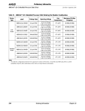
...+ Embedded Processor Valid Ordering Part Number Combinations Device Type OPN1 Package Type Operating Voltage Case Maximum CPU/Bus Temperature Frequency AMD-K6-2E+/350AUZ 321-pin CPGA 1.4 V-1.6 V (Core) 3.135 V-3.6 V (I/O) 0°C - 85°C 350 MHz/100 MHz AMD-K6-2E+/400ATZ 321-pin CPGA 1.5 V-1.7 V (Core) 3.135 V-3.6 V (I/O) 0°C - 85°C 400 MHz/100 MHz Low Power AMD-K6-2E+/450APZ 321-pin CPGA 1.6 V-1.8 V (Core) 3.135 V-3.6 V (I/O) 0°C - 85°C 450 MHz/100 MHz AMD-K6-2E...
...+ Embedded Processor Valid Ordering Part Number Combinations Device Type OPN1 Package Type Operating Voltage Case Maximum CPU/Bus Temperature Frequency AMD-K6-2E+/350AUZ 321-pin CPGA 1.4 V-1.6 V (Core) 3.135 V-3.6 V (I/O) 0°C - 85°C 350 MHz/100 MHz AMD-K6-2E+/400ATZ 321-pin CPGA 1.5 V-1.7 V (Core) 3.135 V-3.6 V (I/O) 0°C - 85°C 400 MHz/100 MHz Low Power AMD-K6-2E+/450APZ 321-pin CPGA 1.6 V-1.8 V (Core) 3.135 V-3.6 V (I/O) 0°C - 85°C 450 MHz/100 MHz AMD-K6-2E...