Service Manual
Page 12
... le numéro spécifié. • U : B+ Line. • V : B- NOTE FOR PRINTED WIRING BOARDS AND SCHEMATIC DIAGRAMS Note on Printed Wiring Board: • X : parts extracted from the component side. • Y : parts extracted from the side ...other layers' patterns are not indicated except for safety. Note on the conductor side. • b : Pattern from the conductor side. • x : parts mounted on Schematic Diagram: • All capacitors are in Ω and 1/4 W or less unless otherwise specified. • f : internal component. • 2 : nonflammable resistor. &#...
... le numéro spécifié. • U : B+ Line. • V : B- NOTE FOR PRINTED WIRING BOARDS AND SCHEMATIC DIAGRAMS Note on Printed Wiring Board: • X : parts extracted from the component side. • Y : parts extracted from the side ...other layers' patterns are not indicated except for safety. Note on the conductor side. • b : Pattern from the conductor side. • x : parts mounted on Schematic Diagram: • All capacitors are in Ω and 1/4 W or less unless otherwise specified. • f : internal component. • 2 : nonflammable resistor. &#...
Service Manual
Page 45
...1. Schematic Diagram - Printed Wiring Board - PANEL Section 30 7-14. ELECTRICAL PARTS LIST 44 SAFETY-RELATED COMPONENT WARNING!! OR DOTTED LINE WITH MARK ! REPLACE THESE COMPONENTS WITH SONY PARTS WHOSE PART NUMBERS APPEAR AS SHOWN IN THIS MANUAL OR IN SUPPLEMENTS PUBLISHED BY SONY. ... disconnected chip component. • Notice that the minus side of emitting radiation exceeding the limit for Printed Wiring Boards and Schematic Diagrams 19 7-2. NOTES ON LASER DIODE EMISSION CHECK The laser beam on the conductor when soldering or unsoldering. Therefore, when...
...1. Schematic Diagram - Printed Wiring Board - PANEL Section 30 7-14. ELECTRICAL PARTS LIST 44 SAFETY-RELATED COMPONENT WARNING!! OR DOTTED LINE WITH MARK ! REPLACE THESE COMPONENTS WITH SONY PARTS WHOSE PART NUMBERS APPEAR AS SHOWN IN THIS MANUAL OR IN SUPPLEMENTS PUBLISHED BY SONY. ... disconnected chip component. • Notice that the minus side of emitting radiation exceeding the limit for Printed Wiring Boards and Schematic Diagrams 19 7-2. NOTES ON LASER DIODE EMISSION CHECK The laser beam on the conductor when soldering or unsoldering. Therefore, when...
Service Manual
Page 62
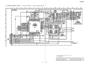
.... Note: Les composants identifiés par une marque 0 sont critiques pour la sécurité. NOTE FOR PRINTED WIRING BOARDS AND SCHEMATIC DIAGRAMS (In addition to this, the necessary note is printed in each block) Note on Printed Wiring Board: • X : parts... otherwise noted. Ne les remplacer que par une pièce portant le numéro spécifié. • U : B+ Line. • V : B- Parts on Schematic Diagram: • All capacitors are taken with a oscilloscope. E : TAPE PLAYBACK (DECK A) d : TAPE PLAYBACK (DECK B) G : RECORD J : CD PLAY (ANALOG OUT) c ...
.... Note: Les composants identifiés par une marque 0 sont critiques pour la sécurité. NOTE FOR PRINTED WIRING BOARDS AND SCHEMATIC DIAGRAMS (In addition to this, the necessary note is printed in each block) Note on Printed Wiring Board: • X : parts... otherwise noted. Ne les remplacer que par une pièce portant le numéro spécifié. • U : B+ Line. • V : B- Parts on Schematic Diagram: • All capacitors are taken with a oscilloscope. E : TAPE PLAYBACK (DECK A) d : TAPE PLAYBACK (DECK B) G : RECORD J : CD PLAY (ANALOG OUT) c ...
Service Manual
Page 64
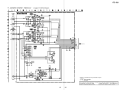
Replace only with respect to ground under no mark : CD PLAY The components identified by mark 0 or dotted line with mark 0 are dc with part number specified. 7-3. no -signal conditions. Ne les remplacer que par une pièce portant le numéro spécifié. BD Board - • See page 32 for Waveforms. • See page 32 for IC Block Diagrams. HTC-NX1 (Page 29) 21 21 • Voltages and waveforms are critical for safety. SCHEMATIC DIAGRAM - Les composants identifiés par une marque 0 sont critiques pour la sécurité.
Replace only with respect to ground under no mark : CD PLAY The components identified by mark 0 or dotted line with mark 0 are dc with part number specified. 7-3. no -signal conditions. Ne les remplacer que par une pièce portant le numéro spécifié. BD Board - • See page 32 for Waveforms. • See page 32 for IC Block Diagrams. HTC-NX1 (Page 29) 21 21 • Voltages and waveforms are critical for safety. SCHEMATIC DIAGRAM - Les composants identifiés par une marque 0 sont critiques pour la sécurité.
Service Manual
Page 66
7-5. SCHEMATIC DIAGRAM - no -signal conditions. CD MOTOR/SENSOR Section - • See page 33 for IC Block Diagram. • Voltages are dc with respect to ground under no mark : CD PLAY HTC-NX1 (Page 29) 23 23 (Page 29)
7-5. SCHEMATIC DIAGRAM - no -signal conditions. CD MOTOR/SENSOR Section - • See page 33 for IC Block Diagram. • Voltages are dc with respect to ground under no mark : CD PLAY HTC-NX1 (Page 29) 23 23 (Page 29)
Service Manual
Page 68
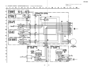
... A +7.5V APB-LCH APB-RCH AGND BPB-LCH BPB-RCH A -7.5V D (Page 28) -VBIAS (-7.5V) +VBIAS (+7.5V) B-REC-RCH B-REC-LCH TC-HEAD-GND HTC-NX1 REC BIAS (R) (DECK B) REC BIAS (L) (DECK B) BIAS OSC REC BIAS -6.8 25 25 • Voltages are dc with part number specified. Ne les remplacer que par...
... A +7.5V APB-LCH APB-RCH AGND BPB-LCH BPB-RCH A -7.5V D (Page 28) -VBIAS (-7.5V) +VBIAS (+7.5V) B-REC-RCH B-REC-LCH TC-HEAD-GND HTC-NX1 REC BIAS (R) (DECK B) REC BIAS (L) (DECK B) BIAS OSC REC BIAS -6.8 25 25 • Voltages are dc with part number specified. Ne les remplacer que par...
Service Manual
Page 69
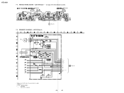
HTC-NX1 7-8. CAPM+ CAPM-H/L A-TRGM TRGM-GND B-TRGM A-SHUT DGND A-HALF +5V A-120/70 B-SHUT A PLAY B-HALF / REC-A / REC-B B-120/70 B PALY NC E (Page 28) • Voltages ...) 05 (DECK A HALF) DECK A PLUNGER (DECK A 120/70) ( ) (DECK A REC) DECK B PLUNGER 4 3 (DECK B PLAY) 1 2 (DECK B REC) (DECK B 120/70) (DECK B HALF) 21 21 L (Page 27) 7-9. SCHEMATIC DIAGRAM - no -signal conditions. LEAF SW Board - (CAPSTAN) CONTROL SWITCH DECK B PLUNGER DECK A PLUNGER (DECK A 120/70) (DECK A HALF) (DECK A REC) (DECK B HALF) (DECK B REC...
HTC-NX1 7-8. CAPM+ CAPM-H/L A-TRGM TRGM-GND B-TRGM A-SHUT DGND A-HALF +5V A-120/70 B-SHUT A PLAY B-HALF / REC-A / REC-B B-120/70 B PALY NC E (Page 28) • Voltages ...) 05 (DECK A HALF) DECK A PLUNGER (DECK A 120/70) ( ) (DECK A REC) DECK B PLUNGER 4 3 (DECK B PLAY) 1 2 (DECK B REC) (DECK B 120/70) (DECK B HALF) 21 21 L (Page 27) 7-9. SCHEMATIC DIAGRAM - no -signal conditions. LEAF SW Board - (CAPSTAN) CONTROL SWITCH DECK B PLUNGER DECK A PLUNGER (DECK A 120/70) (DECK A HALF) (DECK A REC) (DECK B HALF) (DECK B REC...
Service Manual
Page 72
7-12. no mark : CD PLAY ( ) : TAPE PLAYBACK (DECK A) [ ] : TAPE PLAYBACK (DECK B) RECORD ∗ : Impossible to ground under no-signal conditions. MAIN Board (2/2) - • See page 32 for Waveform. (Page 28) HTC-NX1 (Page 23) (Page 23) (Page 21) (Page 31) (Page 31) (Page 31) 29 29 • Voltages and waveforms are dc with respect to measure SCHEMATIC DIAGRAM -
7-12. no mark : CD PLAY ( ) : TAPE PLAYBACK (DECK A) [ ] : TAPE PLAYBACK (DECK B) RECORD ∗ : Impossible to ground under no-signal conditions. MAIN Board (2/2) - • See page 32 for Waveform. (Page 28) HTC-NX1 (Page 23) (Page 23) (Page 21) (Page 31) (Page 31) (Page 31) 29 29 • Voltages and waveforms are dc with respect to measure SCHEMATIC DIAGRAM -

Service Manual
Page 74
7-14. no -signal conditions. PANEL Section - (Page 29) (Page 29) (Page 29) HTC-NX1 31 31 • Voltages are dc with respect to ground under no mark : CD PLAY SCHEMATIC DIAGRAM -
7-14. no -signal conditions. PANEL Section - (Page 29) (Page 29) (Page 29) HTC-NX1 31 31 • Voltages are dc with respect to ground under no mark : CD PLAY SCHEMATIC DIAGRAM -


