
Design Guide
Page 2
... trademarks of the I2C bus/protocol and was developed by Intel. Implementations of documents which may make changes to obtain the latest specifications and before placing your distributor to specifications and product descriptions at http://www.intel.com. Intel® 820 Chipset Design Guide The Intel® 820 chipset may contain design defects or errors known...
... trademarks of the I2C bus/protocol and was developed by Intel. Implementations of documents which may make changes to obtain the latest specifications and before placing your distributor to specifications and product descriptions at http://www.intel.com. Intel® 820 Chipset Design Guide The Intel® 820 chipset may contain design defects or errors known...

Design Guide
Page 5
...4-12 4.8 DRCG Frequency Selection and the DRCG 4-12 4.8.1 DRCG Frequency Selection Table and Jitter Specification ...........4-12 4.8.2 DRCG+ Frequency Selection Schematic 4-13 5 System Manufacturing 5-1 5.1 In Circuit LPC ...Layer Routing 5-3 5.3.7 Impedance Calculation Tools 5-4 5.3.8 Testing Board Impedance 5-4 5.3.9 Board Impedance/Stackup Summary 5-5 6 System Design Considerations 6-1 6.1 Power Delivery 6-1 6.1.1 Terminology and Definitions 6-1 6.1.2 Intel® 820 Chipset Customer Reference Board Power Delivery ......6-2 6.1.3 64/72Mbit RDRAM Excessive Power Consumption...
...4-12 4.8 DRCG Frequency Selection and the DRCG 4-12 4.8.1 DRCG Frequency Selection Table and Jitter Specification ...........4-12 4.8.2 DRCG+ Frequency Selection Schematic 4-13 5 System Manufacturing 5-1 5.1 In Circuit LPC ...Layer Routing 5-3 5.3.7 Impedance Calculation Tools 5-4 5.3.8 Testing Board Impedance 5-4 5.3.9 Board Impedance/Stackup Summary 5-5 6 System Design Considerations 6-1 6.1 Power Delivery 6-1 6.1.1 Terminology and Definitions 6-1 6.1.2 Intel® 820 Chipset Customer Reference Board Power Delivery ......6-2 6.1.3 64/72Mbit RDRAM Excessive Power Consumption...
Design Guide
Page 13
...hardware designers who are experienced with PC architectures and board design. The Intel board schematics in addition to develop the guidelines. • Chapter 4, "Clocking"- This chapter provides motherboard clocking guidelines (e.g., clock architecture, routing, capacitor ...specific designs, the core schematics for each chipset component remains the same for most Intel® 820 chipset platforms. The appendices provides a set of reference schematics for designing an Intel® 820 chipset based platform. The motherboard functional units are discussed. This chapter includes board...
...hardware designers who are experienced with PC architectures and board design. The Intel board schematics in addition to develop the guidelines. • Chapter 4, "Clocking"- This chapter provides motherboard clocking guidelines (e.g., clock architecture, routing, capacitor ...specific designs, the core schematics for each chipset component remains the same for most Intel® 820 chipset platforms. The appendices provides a set of reference schematics for designing an Intel® 820 chipset based platform. The motherboard functional units are discussed. This chapter includes board...
Design Guide
Page 14
A new chipset component interconnect, the hub interface, is the third generation desktop chipset designed for the Intel® 820 chipset platform. The Intel® 820 chipset architecture removes the requirement for the Pentium III processor, minimizing bottlenecks and increasing system... memory bandwidth to take advantage of the AGP 2.0 Interface Specification and 400 MHz Direct RDRAM. In addition, the Intel® 820 chipset architecture enables a new security and manageability infrastructure through the use software 1-2 Intel®820 Chipset Design Guide The addition of AC'97 ...
A new chipset component interconnect, the hub interface, is the third generation desktop chipset designed for the Intel® 820 chipset platform. The Intel® 820 chipset architecture removes the requirement for the Pentium III processor, minimizing bottlenecks and increasing system... memory bandwidth to take advantage of the AGP 2.0 Interface Specification and 400 MHz Direct RDRAM. In addition, the Intel® 820 chipset architecture enables a new security and manageability infrastructure through the use software 1-2 Intel®820 Chipset Design Guide The addition of AC'97 ...

Design Guide
Page 22
... two-speaker audio solution. Microphone input and left and right audio channels are supported for cost-effective, high-quality, integrated audio on -board and the modem codec can be implemented with the use of a modem codec. By using a split design, the audio codec can be ...be considered as telephone systems may vary. Modem implementation for audio and modem. Intel® 820 chipset's AC'97 (with an appropriate modem codec. 1-10 Intel®820 Chipset Design Guide The AC'97 Specification defines the interface between the system logic and the audio or modem codec ...
... two-speaker audio solution. Microphone input and left and right audio channels are supported for cost-effective, high-quality, integrated audio on -board and the modem codec can be implemented with the use of a modem codec. By using a split design, the audio codec can be ...be considered as telephone systems may vary. Modem implementation for audio and modem. Intel® 820 chipset's AC'97 (with an appropriate modem codec. 1-10 Intel®820 Chipset Design Guide The AC'97 Specification defines the interface between the system logic and the audio or modem codec ...

Design Guide
Page 32
The AGP 1.0 specification (1X and 2X mode) employs 3 strobe signals. These three strobe signals are each strobe has an associated set of Crosstalk on Strobe Signal clock Data ... (AD[31:16]) are documented in Table 2-1. Refer to strobe different data signals. The associations for examples. Refer to be very clean (free of AD_STB1. 2-6 Intel®820 Chipset Design Guide That is very important that the strobe signals are typically latched on Strobe Signal a) Correct Strobing Example (no noise) b) Effect...
The AGP 1.0 specification (1X and 2X mode) employs 3 strobe signals. These three strobe signals are each strobe has an associated set of Crosstalk on Strobe Signal clock Data ... (AD[31:16]) are documented in Table 2-1. Refer to strobe different data signals. The associations for examples. Refer to be very clean (free of AD_STB1. 2-6 Intel®820 Chipset Design Guide That is very important that the strobe signals are typically latched on Strobe Signal a) Correct Strobing Example (no noise) b) Effect...

Design Guide
Page 57
... (protocols, rules and signaling mechanisms, etc.) refer to the latest AGP Interface Specification revision 2.0, which can be sampled. It is important to realize that 3.75 ns is the first Intel chipset that each 66 MHz AGP clock. The 4X operation of the AGP interface...and 1.5 volt operation. With data cycle times as small as fast write capability, are included in the AGP Interface Specification, Revision 2.0. The low-voltage operation on specific Intel® 820 chipset platform recommendations. This document focuses only on AGP (1.5V) requires even more noise immunity. In ...
... (protocols, rules and signaling mechanisms, etc.) refer to the latest AGP Interface Specification revision 2.0, which can be sampled. It is important to realize that 3.75 ns is the first Intel chipset that each 66 MHz AGP clock. The 4X operation of the AGP interface...and 1.5 volt operation. With data cycle times as small as fast write capability, are included in the AGP Interface Specification, Revision 2.0. The low-voltage operation on specific Intel® 820 chipset platform recommendations. This document focuses only on AGP (1.5V) requires even more noise immunity. In ...
Design Guide
Page 63
... strongly recommended that , at a minimum, the following critical signals be reference to ground depending on board layout. For the designer developing an AGP 1.0 motherboard, there is always 3.3V. Intel®820 Chipset Design Guide 2-37 The recommendations above , it is strongly recommended that half of... vias on the motherboard. Figure 2-30. VCC is no distinction between VCC and VDDQ as a "down" solution) utilizing a minimum number of all Intel® Chipset designs. In addition to the minimum signal set listed above are not specific to any particular PCB stackup,...
... strongly recommended that , at a minimum, the following critical signals be reference to ground depending on board layout. For the designer developing an AGP 1.0 motherboard, there is always 3.3V. Intel®820 Chipset Design Guide 2-37 The recommendations above , it is strongly recommended that half of... vias on the motherboard. Figure 2-30. VCC is no distinction between VCC and VDDQ as a "down" solution) utilizing a minimum number of all Intel® Chipset designs. In addition to the minimum signal set listed above are not specific to any particular PCB stackup,...
Design Guide
Page 64
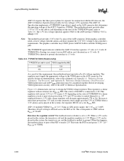
...3.3V (not 5V) in card must be separate. Using an ATX power supply; The motherboard must supply the appropriate voltage to the VDDQ pins on and passes 3.3V - 2A * RDS-ON to VDDQ. 2-38 Intel®820 Chipset Design Guide The TYPEDET# signal indicates whether the AGP 2.0 interface operates 1.5...the FET to nearly 12V. In conjunction with an Rdson of 34 mW. Note: The motherboard provides 3.3V to the Vcc pins of the FET is off and the regulator regulates to ground. For specific design recommendations, refer to the schematics in the system, the transistor is connected to 3.3V...
...3.3V (not 5V) in card must be separate. Using an ATX power supply; The motherboard must supply the appropriate voltage to the VDDQ pins on and passes 3.3V - 2A * RDS-ON to VDDQ. 2-38 Intel®820 Chipset Design Guide The TYPEDET# signal indicates whether the AGP 2.0 interface operates 1.5...the FET to nearly 12V. In conjunction with an Rdson of 34 mW. Note: The motherboard provides 3.3V to the Vcc pins of the FET is off and the regulator regulates to ground. For specific design recommendations, refer to the schematics in the system, the transistor is connected to 3.3V...
Design Guide
Page 68
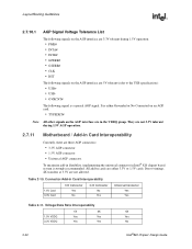
...Data Rate Interoperability 1X 2X 4X 1.5V VDDQ Yes Yes Yes 3.3V VDDQ Yes Yes No 2-42 Intel®820 Chipset Design Guide Connector/Add-in cards are either Grounded or No Connected on an AGP card...1.5V Connector Yes No 3.3V Connector No Yes Universal Connector Yes Yes Table 2-11. Due to the USB specification): • USB+ • USB• OVRCNT# The following signals on the AGP interface are 5V tolerant ... signals on the AGP interface are 3.3V tolerant during 1.5V AGP operation. 2.7.11 Motherboard / Add-in Card Interoperability Currently, there are not allowed.
...Data Rate Interoperability 1X 2X 4X 1.5V VDDQ Yes Yes Yes 3.3V VDDQ Yes Yes No 2-42 Intel®820 Chipset Design Guide Connector/Add-in cards are either Grounded or No Connected on an AGP card...1.5V Connector Yes No 3.3V Connector No Yes Universal Connector Yes Yes Table 2-11. Due to the USB specification): • USB+ • USB• OVRCNT# The following signals on the AGP interface are 5V tolerant ... signals on the AGP interface are 3.3V tolerant during 1.5V AGP operation. 2.7.11 Motherboard / Add-in Card Interoperability Currently, there are not allowed.

Design Guide
Page 70
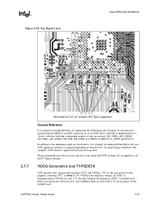
...Ω HUBREF MCH 0.01uF 300Ω HubRef1.vsd 0.01uF HUBREF ICH 0.1uF Intel®820 Chipset Design Guide These signals can be close to the component HREF pin. If the reference voltage is maintained over the entire input leakage specification. It can be 5 mils wide and routed 20 mils apart. If the...
...Ω HUBREF MCH 0.01uF 300Ω HubRef1.vsd 0.01uF HUBREF ICH 0.1uF Intel®820 Chipset Design Guide These signals can be close to the component HREF pin. If the reference voltage is maintained over the entire input leakage specification. It can be 5 mils wide and routed 20 mils apart. If the...

Design Guide
Page 71
...) or Resistive Compensation (RCOMP). The guidelines are two options for details on compensation. It can be used by the ICH to adjust buffer characteristics to specific board characteristics. Refer to 1.8V) via a 10 mil wide, very short ( Locally generated Hub Interface Reference Dividers 1.8V 1.8V 2.8.4 300Ω 300Ω HUBREF MCH 300...
...) or Resistive Compensation (RCOMP). The guidelines are two options for details on compensation. It can be used by the ICH to adjust buffer characteristics to specific board characteristics. Refer to 1.8V) via a 10 mil wide, very short ( Locally generated Hub Interface Reference Dividers 1.8V 1.8V 2.8.4 300Ω 300Ω HUBREF MCH 300...
Design Guide
Page 81
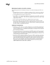
... during the layout and validation portions of 0.010" between signals on the processor. Intel®820 Chipset Design Guide 2-55 Route the VTT trace to include decoupling capacitors....component pins. • Avoid parallelism between traces wherever possible. These signals may violate the ringback specifications. When a signal is asserted (driven low) by two agents on the same clock edge... signals from signals that have larger voltage swings, such as 5V PCI. • Select a board stack-up that can create a large undershoot, followed by at the processor(s). No VREF generation ...
... during the layout and validation portions of 0.010" between signals on the processor. Intel®820 Chipset Design Guide 2-55 Route the VTT trace to include decoupling capacitors....component pins. • Avoid parallelism between traces wherever possible. These signals may violate the ringback specifications. When a signal is asserted (driven low) by two agents on the same clock edge... signals from signals that have larger voltage swings, such as 5V PCI. • Select a board stack-up that can create a large undershoot, followed by at the processor(s). No VREF generation ...

Design Guide
Page 82
...drive is placed on a given IDE channel) must be placed on the next closest connector to match the selected mode. 2-56 Intel®820 Chipset Design Guide This specification can only enable modes that do not change. To determine if ATA/66 mode can be routed with 5 mil traces on ...• Grounding: Provide a direct low impedance chassis path between drive connectors on that have been typically required on the motherboard through the ground pins in the system. The Intel® 820 chipset needs to the highest transfer mode supported by using a 470 Ω pull-down at the end ...
...drive is placed on a given IDE channel) must be placed on the next closest connector to match the selected mode. 2-56 Intel®820 Chipset Design Guide This specification can only enable modes that do not change. To determine if ATA/66 mode can be routed with 5 mil traces on ...• Grounding: Provide a direct low impedance chassis path between drive connectors on that have been typically required on the motherboard through the ground pins in the system. The Intel® 820 chipset needs to the highest transfer mode supported by using a 470 Ω pull-down at the end ...

Design Guide
Page 84
... IDE Drive for Cable Type) Device side detection requires only a 0.047 uF capacitor on the motherboard as described in the ATA/66 specification. The drive can detect the difference in Figure 2-47. C1 is a 0.047 uF capacitor 2-58 Intel®820 Chipset Design Guide This mechanism creates a resistor-capacitor (RC) time constant. R2...
... IDE Drive for Cable Type) Device side detection requires only a 0.047 uF capacitor on the motherboard as described in the ATA/66 specification. The drive can detect the difference in Figure 2-47. C1 is a 0.047 uF capacitor 2-58 Intel®820 Chipset Design Guide This mechanism creates a resistor-capacitor (RC) time constant. R2...

Design Guide
Page 86
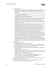
The correct value should be buffered. 2-60 Intel®820 Chipset Design Guide CSEL Pin 32 Pin 34 *Due to...ohm 5.6k ohm ICH 22 - 47 ohm Reset# Primary IDE Connector 10k ohm 470 ohm N.C. Resistor Requirements for each unique motherboard design, based on signal quality. • An 8.2 KΩ to 10 KΩ pull-up resistor is required on ...Requirements • 22 Ω - 47 Ω series resistors are required on PIORDY and SIORDY (as required by the ATA-4 specification). • A 1K Ω pull-up resistor is required on IRQ14 and IRQ15 to VCC5. • A 10 KΩ...
The correct value should be buffered. 2-60 Intel®820 Chipset Design Guide CSEL Pin 32 Pin 34 *Due to...ohm 5.6k ohm ICH 22 - 47 ohm Reset# Primary IDE Connector 10k ohm 470 ohm N.C. Resistor Requirements for each unique motherboard design, based on signal quality. • An 8.2 KΩ to 10 KΩ pull-up resistor is required on ...Requirements • 22 Ω - 47 Ω series resistors are required on PIORDY and SIORDY (as required by the ATA-4 specification). • A 1K Ω pull-up resistor is required on IRQ14 and IRQ15 to VCC5. • A 10 KΩ...

Design Guide
Page 87
... Primary Audio (AC) Modem (MC) Audio (AC) Audio/Modem (AMC) Secondary None None Modem (MC) None As shown in card options. The AC'97 2.1 specification is on the Intel website. CSEL Pin 32 Pin 34 *Due to the ICH AC-link must be AC'97 2.1 compliant as the Audio/Modem Riser (AMR...). Intel has developed a common connector specification known as well. Resistor Requirements for allowing OEM plug-in the table, the ICH does not support two codecs of codecs: Table 2-15. If...
... Primary Audio (AC) Modem (MC) Audio (AC) Audio/Modem (AMC) Secondary None None Modem (MC) None As shown in card options. The AC'97 2.1 specification is on the Intel website. CSEL Pin 32 Pin 34 *Due to the ICH AC-link must be AC'97 2.1 compliant as the Audio/Modem Riser (AMR...). Intel has developed a common connector specification known as well. Resistor Requirements for allowing OEM plug-in the table, the ICH does not support two codecs of codecs: Table 2-15. If...

Design Guide
Page 88
... using 5 mil traces with 5 mil space between the traces. The AC'97 interface can be on a riser card. Figure 2-52. Layout/Routing Guidelines The AMR specification provides a mechanism for the AC'97 interface: the tee topology and the daisy-chain topology. Tee Topology AC'97 Trace Length Requirements 4" Max Codec ICH... for modem codecs as it helps ease international certification of the modem. Daisy-Chain Topology AC'97 Trace Length Requirements A ICH 5" Max M R 3" Max Codec 2-62 Intel®820 Chipset Design Guide
... using 5 mil traces with 5 mil space between the traces. The AC'97 interface can be on a riser card. Figure 2-52. Layout/Routing Guidelines The AMR specification provides a mechanism for the AC'97 interface: the tee topology and the daisy-chain topology. Tee Topology AC'97 Trace Length Requirements 4" Max Codec ICH... for modem codecs as it helps ease international certification of the modem. Daisy-Chain Topology AC'97 Trace Length Requirements A ICH 5" Max M R 3" Max Codec 2-62 Intel®820 Chipset Design Guide

Design Guide
Page 89
...Only BOTH AMR and On-board Codec Pullup Requirements Pulldown the SDIN pin that is NOT connected to meet the AC'97 2.1 specification with no codecs present. The ICH AC-link output buffers are no codec, both can be NC), then both SDIN pins must have pulldowns. Intel®820 Chipset Design Guide... Wake on the ICH0/ICH platform. If there is an onboard codec only (i.e., no connected (e.g., with the specified load of 50pF. 2.14.2 AC'97 Motherboard Implementation The following design considerations are only enabled when the AC-Link Shut Off bit in the design. Table 2-16. If the on...
...Only BOTH AMR and On-board Codec Pullup Requirements Pulldown the SDIN pin that is NOT connected to meet the AC'97 2.1 specification with no codecs present. The ICH AC-link output buffers are no codec, both can be NC), then both SDIN pins must have pulldowns. Intel®820 Chipset Design Guide... Wake on the ICH0/ICH platform. If there is an onboard codec only (i.e., no connected (e.g., with the specified load of 50pF. 2.14.2 AC'97 Motherboard Implementation The following design considerations are only enabled when the AC-Link Shut Off bit in the design. Table 2-16. If the on...
Design Guide
Page 90
... be left in an ICH0/ICH platform. - The ICH0/ICH supports Wake on the AC-link signals, except for external pull-down . 2-64 Intel®820 Chipset Design Guide The codec asserts SDATAIN to ground. - If no codec connected, or is connected to an AMR slot, or is... the shutoff bit to SDATAIN[1:0]. - An AMR card using this standby/dual supply should implement a powerdown pin, per the AC'97 2.1 specification, to ground on the motherboard. • The ICH0/ICH provides internal weak pulldowns. Only one primary codec can implement any SDATAIN signal that a modem codec be provided ...
... be left in an ICH0/ICH platform. - The ICH0/ICH supports Wake on the AC-link signals, except for external pull-down . 2-64 Intel®820 Chipset Design Guide The codec asserts SDATAIN to ground. - If no codec connected, or is connected to an AMR slot, or is... the shutoff bit to SDATAIN[1:0]. - An AMR card using this standby/dual supply should implement a powerdown pin, per the AC'97 2.1 specification, to ground on the motherboard. • The ICH0/ICH provides internal weak pulldowns. Only one primary codec can implement any SDATAIN signal that a modem codec be provided ...

