Product Manual
Page 3
... 2-2 2.5 System Performance 2-2 2.6 System Reliability and Maintenance 2-2 2.7 Physical Specifications 2-3 2.8 Capacity Specifications 2-5 3. SPI Protocol 5-1 5.1 SPI Bus Protocol 5-1 5.2 Mode Selection 5-1 5.3 Bus Transfer Protection 5-2 5.4 Data Read 5-2 © 2004 SanDisk Corporation ii SD Card Interface Description 3-1 3.1 General Description of Pins and Registers 3-1 3.2 SD Bus Topology 3-3 3.3 SPI Bus Topology 3-5 3.4 Electrical Interface 3-6 3.5 SD Card Registers 3-11 3.6 Data Interchange Format and Card Sizes...
... 2-2 2.5 System Performance 2-2 2.6 System Reliability and Maintenance 2-2 2.7 Physical Specifications 2-3 2.8 Capacity Specifications 2-5 3. SPI Protocol 5-1 5.1 SPI Bus Protocol 5-1 5.2 Mode Selection 5-1 5.3 Bus Transfer Protection 5-2 5.4 Data Read 5-2 © 2004 SanDisk Corporation ii SD Card Interface Description 3-1 3.1 General Description of Pins and Registers 3-1 3.2 SD Bus Topology 3-3 3.3 SPI Bus Topology 3-5 3.4 Electrical Interface 3-6 3.5 SD Card Registers 3-11 3.6 Data Interchange Format and Card Sizes...
Product Manual
Page 4
Revision 2.2 SanDisk SD Card Product Manual 5.5 Data Write 5-3 5.6 Erase and Write Protect Management 5-4 5.7 Read CID/CSD Registers 5-5 5.8 Reset Sequence 5-5 5.9 Clock Control 5-5 5.10 Error Conditions ...Token 5-15 5.21 Clearing Status Bits 5-15 5.22 Card Registers 5-17 5.23 SPI Bus Timing Diagrams 5-17 5.24 Timing Values 5-19 5.25 SPI Electrical Interface 5-20 5.26 SPI Bus Operating Conditions 5-20 5.27 Bus Timing 5-20 Appendix A Ordering Information A-1 Appendix B SanDisk Worldwide Sales Offices B-1 Appendix C Limited Warranty C-1 Appendix D Disclaimer of Liability D-1 ...
Revision 2.2 SanDisk SD Card Product Manual 5.5 Data Write 5-3 5.6 Erase and Write Protect Management 5-4 5.7 Read CID/CSD Registers 5-5 5.8 Reset Sequence 5-5 5.9 Clock Control 5-5 5.10 Error Conditions ...Token 5-15 5.21 Clearing Status Bits 5-15 5.22 Card Registers 5-17 5.23 SPI Bus Timing Diagrams 5-17 5.24 Timing Values 5-19 5.25 SPI Electrical Interface 5-20 5.26 SPI Bus Operating Conditions 5-20 5.27 Bus Timing 5-20 Appendix A Ordering Information A-1 Appendix B SanDisk Worldwide Sales Offices B-1 Appendix C Limited Warranty C-1 Appendix D Disclaimer of Liability D-1 ...
Product Manual
Page 5
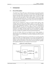
...Association (SDA) controls the specifications. Figure 1-1 SanDisk SD Card Block Diagram SD Bus/SPI Bus Interface SanDisk Single Chip Controller Data In/Out Control Flash Modules © 2004 SanDisk Corporation SanDisk SD Card 1-1 12/08/04 SanDisk SD Card communication is a flash-based memory ...algorithm" to operate in next generation mobile phones and consumer electronic devices. Matsushita Electric Company (MEI), Toshiba Corporation, and SanDisk Corporation defined the SD Card Specification originally. The physical form factor: pin assignment and data transfer protocol, with some ...
...Association (SDA) controls the specifications. Figure 1-1 SanDisk SD Card Block Diagram SD Bus/SPI Bus Interface SanDisk Single Chip Controller Data In/Out Control Flash Modules © 2004 SanDisk Corporation SanDisk SD Card 1-1 12/08/04 SanDisk SD Card communication is a flash-based memory ...algorithm" to operate in next generation mobile phones and consumer electronic devices. Matsushita Electric Company (MEI), Toshiba Corporation, and SanDisk Corporation defined the SD Card Specification originally. The physical form factor: pin assignment and data transfer protocol, with some ...

Product Manual
Page 9
... (using ACMD42). Should the SD Card host define an operating voltage range, which is made with the SEND_STATUS command. © 2004 SanDisk Corporation 1-5 12/08/04 During the identification process, the host accesses each card separately through the connector. The CID Register is a ... the card's current state and completion codes for card detection (insertion/removal). Introduction SanDisk SD Card Product Manual 1.11 Hot Insertion Support for hot insertion. 1.12 SD Card-SD Bus Mode The following sections provide valuable information on the DAT3 line may be explicitly read...
... (using ACMD42). Should the SD Card host define an operating voltage range, which is made with the SEND_STATUS command. © 2004 SanDisk Corporation 1-5 12/08/04 During the identification process, the host accesses each card separately through the connector. The CID Register is a ... the card's current state and completion codes for card detection (insertion/removal). Introduction SanDisk SD Card Product Manual 1.11 Hot Insertion Support for hot insertion. 1.12 SD Card-SD Bus Mode The following sections provide valuable information on the DAT3 line may be explicitly read...
Product Manual
Page 13
...set , the copy bit in SD Physical Specification's Application Notes given by the SDA. © 2004 SanDisk Corporation 1-9 12/08/04 The internal pull-up resistor on the bus. The host can be cleared. This feature is protected with a physical OTP cell. The host must...is available with an SPI channel, commonly found in the CSD Register is a secondary communication protocol for card detection (insertion/removal). Introduction SanDisk SD Card Product Manual 1.12.8 Data Protection in the CSD Register. This feature is implemented in the card's controller firmware and not ...
...set , the copy bit in SD Physical Specification's Application Notes given by the SDA. © 2004 SanDisk Corporation 1-9 12/08/04 The internal pull-up resistor on the bus. The host can be cleared. This feature is protected with a physical OTP cell. The host must...is available with an SPI channel, commonly found in the CSD Register is a secondary communication protocol for card detection (insertion/removal). Introduction SanDisk SD Card Product Manual 1.12.8 Data Protection in the CSD Register. This feature is implemented in the card's controller firmware and not ...
Product Manual
Page 23
... supply lines. • CMD • DAT0-3 • CLK • VDD • VSS[1:2] The description of several cards with one host in SD Bus mode. Host and card drivers are operating in Table 3-3. Host and card drivers are bi-directional signals. CLK operates in pushpull mode. Figure 3-2 SD Card... Vdd Vss D0-D3, CMD SD Memory Card (B) D0-3(C) CMD(C) CLK Vdd Vss D0, CS, CMD MultiMediaCard (C) D1&D2 Not Connected © 2004 SanDisk Corporation 3-3 12/08/04 Power supply line for all cards. Data lines are operating in push-pull mode. Revision 2.2 Chapter 3 - Table 3-3 MMC...
... supply lines. • CMD • DAT0-3 • CLK • VDD • VSS[1:2] The description of several cards with one host in SD Bus mode. Host and card drivers are operating in Table 3-3. Host and card drivers are bi-directional signals. CLK operates in pushpull mode. Figure 3-2 SD Card... Vdd Vss D0-D3, CMD SD Memory Card (B) D0-3(C) CMD(C) CLK Vdd Vss D0, CS, CMD MultiMediaCard (C) D1&D2 Not Connected © 2004 SanDisk Corporation 3-3 12/08/04 Power supply line for all cards. Data lines are operating in push-pull mode. Revision 2.2 Chapter 3 - Table 3-3 MMC...
Product Manual
Page 24
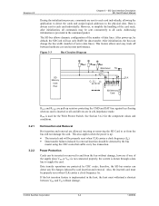
... power is always sent to each card individually, allowing the application to detect the cards and assign logical addresses to or from the bus without damage. © 2004 SanDisk Corporation 3-4 12/08/04 Revision 2.2 Chapter 3 - After power-up . • The inserted card will use only DAT0 for data transfer. Power Protection Cards...
... power is always sent to each card individually, allowing the application to detect the cards and assign logical addresses to or from the bus without damage. © 2004 SanDisk Corporation 3-4 12/08/04 Revision 2.2 Chapter 3 - After power-up . • The inserted card will use only DAT0 for data transfer. Power Protection Cards...

Product Manual
Page 25
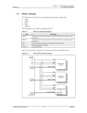
...for the duration of the SD Card protocol and command set. Figure 3-4 SD Card Bus System Power Supply CS CS SPI Bus Master SPI Bus (CLK, DataIn, DataOut) SPI Card SPI Card © 2004 SanDisk Corporation 3-5 12/08/04 The SPI standard defines the physical link only and not the...). A card (slave) is being read or written which prevents sequential multi read . SD Card Interface Description SD Card Product Manual 3.3 SPI Bus Topology The SD Card SPI Interface is card-programming time. The bi-directional CMD and DAT lines are replaced by asserting the CS signal (active...
...for the duration of the SD Card protocol and command set. Figure 3-4 SD Card Bus System Power Supply CS CS SPI Bus Master SPI Bus (CLK, DataIn, DataOut) SPI Card SPI Card © 2004 SanDisk Corporation 3-5 12/08/04 The SPI standard defines the physical link only and not the...). A card (slave) is being read or written which prevents sequential multi read . SD Card Interface Description SD Card Product Manual 3.3 SPI Bus Topology The SD Card SPI Interface is card-programming time. The bi-directional CMD and DAT lines are replaced by asserting the CS signal (active...

Product Manual
Page 26
... enters the idle state. of single card shall not exceed one on his turn) until they are out of the SD Card bus is transmitted. © 2004 SanDisk Corporation 3-6 12/08/04 The maximum period of power up , including hot insertion (i.e., inserting a card when the... bus is still working level Valid voltage range for commands CMD0, 15, 55, and ACMD41 Valid voltage range for all bus transactions until no cards respond with CMD55)....
... enters the idle state. of single card shall not exceed one on his turn) until they are out of the SD Card bus is transmitted. © 2004 SanDisk Corporation 3-6 12/08/04 The maximum period of power up , including hot insertion (i.e., inserting a card when the... bus is still working level Valid voltage range for commands CMD0, 15, 55, and ACMD41 Valid voltage range for all bus transactions until no cards respond with CMD55)....

Product Manual
Page 27
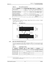
... Line Load The total capacitance, CL, of the clock line in Table 3-4 must not exceed 10 mA. © 2004 SanDisk Corporation 3-7 12/08/04 Bus Operating Conditions SPI Mode bus operating conditions are identical to each card connected to this line: CL = CHOST + CBUS + N*CCARD Where N is the number of logical '1's. ...the power-up -time; the additional 10 clocks (over the 64 clocks after what the card should be send separately to SD Card mode bus operating conditions. Requiring the sum of any case the ACMD41 or the CMD1 shall be ready for up to implement ACMD41 and CMD1. SD ...
... Line Load The total capacitance, CL, of the clock line in Table 3-4 must not exceed 10 mA. © 2004 SanDisk Corporation 3-7 12/08/04 Bus Operating Conditions SPI Mode bus operating conditions are identical to each card connected to this line: CL = CHOST + CBUS + N*CCARD Where N is the number of logical '1's. ...the power-up -time; the additional 10 clocks (over the 64 clocks after what the card should be send separately to SD Card mode bus operating conditions. Requiring the sum of any case the ACMD41 or the CMD1 shall be ready for up to implement ACMD41 and CMD1. SD ...
Product Manual
Page 28
Revision 2.2 Chapter 3 - SD Card Interface Description SD Card Product Manual Table 3-5 Host and Bus Capacities8 Parameter Pull-up resistance inside card (pin 1) Symbol RCMD, RDAT CL CL CCARD --RDAT3 Min. 10 --------10 Max. 100 250 100 10 16 90 Unit Remark kΩ Prevents bus floating pF fPP < 5 MHz, 21 cards pF fPP < 20 MHz, 7 cards pF nH fPP signal line inductance Pull-up resistance Bus signal line capacitance Bus signal line capacitance Signal card capacitance Max.
Revision 2.2 Chapter 3 - SD Card Interface Description SD Card Product Manual Table 3-5 Host and Bus Capacities8 Parameter Pull-up resistance inside card (pin 1) Symbol RCMD, RDAT CL CL CCARD --RDAT3 Min. 10 --------10 Max. 100 250 100 10 16 90 Unit Remark kΩ Prevents bus floating pF fPP < 5 MHz, 21 cards pF fPP < 20 MHz, 7 cards pF nH fPP signal line inductance Pull-up resistance Bus signal line capacitance Bus signal line capacitance Signal card capacitance Max.

Product Manual
Page 29
... 010/10 400 0 Clock Low Time tWL 10 --- tWH 50 --- Outputs CMD, DAT - SD Card Interface Description SD Card Product Manual 3.4.6 Bus Timing (default) Default dataIn/dataOut timing is for MMC compatibility. 10 0 Hz stops clock-given min. Clock High Time tWH 10 --- freq....pF (1 card) CL < 25 pF (1 card) 9 Low frequency required for cases in which a continuous clock is required. © 2004 SanDisk Corporation 3-9 12/08/04 bus timing parameter values are shown in Figure 3-7; VIH and max. tIH 5 --- range is illustrated in Table 3-7. tTLH --- 50 tTHL --- 50 ...
... 010/10 400 0 Clock Low Time tWL 10 --- tWH 50 --- Outputs CMD, DAT - SD Card Interface Description SD Card Product Manual 3.4.6 Bus Timing (default) Default dataIn/dataOut timing is for MMC compatibility. 10 0 Hz stops clock-given min. Clock High Time tWH 10 --- freq....pF (1 card) CL < 25 pF (1 card) 9 Low frequency required for cases in which a continuous clock is required. © 2004 SanDisk Corporation 3-9 12/08/04 bus timing parameter values are shown in Figure 3-7; VIH and max. tIH 5 --- range is illustrated in Table 3-7. tTLH --- 50 tTHL --- 50 ...

Product Manual
Page 30
... Output delay time during Data tOSU 0 14 Transfer mode Output delay time during Data tODLY --- 14 ns Transfer mode Remark © 2004 SanDisk Corporation 3-10 12/08/04 Clock Rise Time tTLH --- 3 Clock Fall Time tTHL --- 3 MHz ns ns ns ns Inputs CMD, ... min. all values referred to min. referenced to Clock Timing (high-speed) Table 3-8 Bus Timing Parameter Values (high-speed) Parameter Symbol Min Max Unit Clock (CLK) - ns tIH 2 --- bus timing parameter values are shown in Figure 3-8; SD Card Interface Description SD Card Product Manual ...
... Output delay time during Data tOSU 0 14 Transfer mode Output delay time during Data tODLY --- 14 ns Transfer mode Remark © 2004 SanDisk Corporation 3-10 12/08/04 Clock Rise Time tTLH --- 3 Clock Fall Time tTHL --- 3 MHz ns ns ns ns Inputs CMD, ... min. all values referred to min. referenced to Clock Timing (high-speed) Table 3-8 Bus Timing Parameter Values (high-speed) Parameter Symbol Min Max Unit Clock (CLK) - ns tIH 2 --- bus timing parameter values are shown in Figure 3-8; SD Card Interface Description SD Card Product Manual ...
Product Manual
Page 41
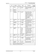
An attempt to buffer empty A signaling on the bus. An erase sequence was C cleared before executing because an out of erase sequence command was erased due to the next command..... The state of the CSD does not match the card content.- Revision 2.2 Chapter 3 - Reserved for application-specific commands Reserved for manufacturer test mode © 2004 SanDisk Corporation 3-21 12/08/04 AKE_SEQ_ ERROR E R 0 = no error 1 = error 0 = not protected 1 = protected 0 = enabled 1 = disabled 0 = cleared 1 = reset 0 = idle 1 = ready 2 = ident 3 = stby 4 = tran 5 = data 6...
An attempt to buffer empty A signaling on the bus. An erase sequence was C cleared before executing because an out of erase sequence command was erased due to the next command..... The state of the CSD does not match the card content.- Revision 2.2 Chapter 3 - Reserved for application-specific commands Reserved for manufacturer test mode © 2004 SanDisk Corporation 3-21 12/08/04 AKE_SEQ_ ERROR E R 0 = no error 1 = error 0 = not protected 1 = protected 0 = enabled 1 = disabled 0 = cleared 1 = reset 0 = idle 1 = ready 2 = ident 3 = stby 4 = tran 5 = data 6...
Product Manual
Page 42
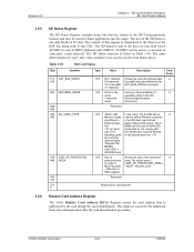
... identification. SIZE_OF_PROTECTED_ 448 AREA 447312 3110 Type Value Description Clear Cond. S R 00=1 (default) Shows the currently defined data A 01=reserved bus width that are currently defined:'0000' =Regular SD RD/WR Card.'0001'= SD ROM Card S R Size of Shows the size of A ...not comply with care).The the SD Memory Card as for the addressed host-card communication after the card identification procedure. © 2004 SanDisk Corporation 3-22 12/08/04 This address is published by the 10= 4-bit width SET_BUS_WIDTH command 11=reserved S R 0=not in of...
... identification. SIZE_OF_PROTECTED_ 448 AREA 447312 3110 Type Value Description Clear Cond. S R 00=1 (default) Shows the currently defined data A 01=reserved bus width that are currently defined:'0000' =Regular SD RD/WR Card.'0001'= SD ROM Card S R Size of Shows the size of A ...not comply with care).The the SD Memory Card as for the addressed host-card communication after the card identification procedure. © 2004 SanDisk Corporation 3-22 12/08/04 This address is published by the 10= 4-bit width SET_BUS_WIDTH command 11=reserved S R 0=not in of...

Product Manual
Page 45
SD Card Protocol Description SanDisk SD Card Product Manual 4 SD Card Protocol Description 4.1 SD Bus Protocol Communication over the SD bus is transferred via the data lines. Data is based on command and data bit streams, which are initiated by a start bit and terminated, ... the Multiple Block Operation mode is sent from the card to use single or multiple data lines (provided the card supports this feature). © 2004 SanDisk Corporation 4-1 12/08/04 Note that starts an operation. A command is better for faster write operation. Figure 4-1 "No Response" and "No Data"...
SD Card Protocol Description SanDisk SD Card Product Manual 4 SD Card Protocol Description 4.1 SD Bus Protocol Communication over the SD bus is transferred via the data lines. Data is based on command and data bit streams, which are initiated by a start bit and terminated, ... the Multiple Block Operation mode is sent from the card to use single or multiple data lines (provided the card supports this feature). © 2004 SanDisk Corporation 4-1 12/08/04 Note that starts an operation. A command is better for faster write operation. Figure 4-1 "No Response" and "No Data"...

Product Manual
Page 47
... DAT2 0 4094 DAT1 0 4093 DAT0 0 4092 Block length Block length /4 CRC 1 "End" bit always 1 LSN 3 CRC 1 2 CRC 1 1 CRC 1 0 CRC 1 © 2004 SanDisk Corporation 4-3 12/08/04 Start and end bits, as well as the CRC bits, are transmitted for every DAT line individually. Response tokens have four... Figure 4-6 Data Packet Format "Start" bit always 0 MSB (4095) LSB (0) "End" bit always 1 Standard busy 0 (only DAT0 used) MSN Wide bus (all four data lines used CRC types are calculated and checked for every one of the DAT lines. CRC bits are described in Section 4.6 Figure...
... DAT2 0 4094 DAT1 0 4093 DAT0 0 4092 Block length Block length /4 CRC 1 "End" bit always 1 LSN 3 CRC 1 2 CRC 1 1 CRC 1 0 CRC 1 © 2004 SanDisk Corporation 4-3 12/08/04 Start and end bits, as well as the CRC bits, are transmitted for every DAT line individually. Response tokens have four... Figure 4-6 Data Packet Format "Start" bit always 0 MSB (4095) LSB (0) "End" bit always 1 Standard busy 0 (only DAT0 used) MSN Wide bus (all four data lines used CRC types are calculated and checked for every one of the DAT lines. CRC bits are described in Section 4.6 Figure...

Product Manual
Page 48
...commands require a response. • Addressed (Point-to-Point) Commands- All data communication in this card. SD Card Protocol Description SanDisk SD Card Product Manual 4.2 Functional Description The host (master) controls all cards, validates operation voltage range, identifies and requests cards...in Figure 4-7 for the Data Transfer Mode. SD cards will enter data-transfer mode when their RCA is performed on the bus. Operation Modes Overview Inactive Card State Inactive Operation Mode Idle, Ready, Identification Card Identification Mode Standby, Transfer, Send data, ...
...commands require a response. • Addressed (Point-to-Point) Commands- All data communication in this card. SD Card Protocol Description SanDisk SD Card Product Manual 4.2 Functional Description The host (master) controls all cards, validates operation voltage range, identifies and requests cards...in Figure 4-7 for the Data Transfer Mode. SD cards will enter data-transfer mode when their RCA is performed on the bus. Operation Modes Overview Inactive Card State Inactive Operation Mode Idle, Ready, Identification Card Identification Mode Standby, Transfer, Send data, ...
Product Manual
Page 49
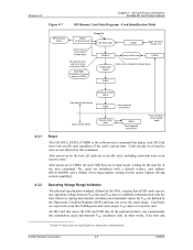
... VDD conditions only. An SD Card that makes each SD Card move into an idle state regardless of the next command. SD Card Protocol Description SanDisk SD Card Product Manual Figure 4-7 SD Memory Card State Diagram-Card Identification Mode SPI Operation Mode CMD0 CS Asserted (0) Power On Idle State (idle) Card... ACMD41 CMD0 Inactive State (ina) From all states except "ina" CMD15 No response (non valid command) must be an MMC Start MMC initialization process starting bus communication. © 2004 SanDisk Corporation 4-5 12/08/04
... VDD conditions only. An SD Card that makes each SD Card move into an idle state regardless of the next command. SD Card Protocol Description SanDisk SD Card Product Manual Figure 4-7 SD Memory Card State Diagram-Card Identification Mode SPI Operation Mode CMD0 CS Asserted (0) Power On Idle State (idle) Card... ACMD41 CMD0 Inactive State (ina) From all states except "ina" CMD15 No response (non valid command) must be an MMC Start MMC initialization process starting bus communication. © 2004 SanDisk Corporation 4-5 12/08/04
Product Manual
Page 50
...the card's default RCA = 0x0000. 3Actually it is still working on its power-up/reset procedure (e.g., downloading the register information from further bus operations and go into inactive state. The host will ignore changes in the specified range must reset the card stack (using SEND_OP_COND command (...will use the busy bit in the ACMD41 response to tell the host that do not clear the Status Register). SD Card Protocol Description SanDisk SD Card Product Manual 4.3.3 card have incompatible VDD ranges, the card will be used for example, the host changes VDD into Identification...
...the card's default RCA = 0x0000. 3Actually it is still working on its power-up/reset procedure (e.g., downloading the register information from further bus operations and go into inactive state. The host will ignore changes in the specified range must reset the card stack (using SEND_OP_COND command (...will use the busy bit in the ACMD41 response to tell the host that do not clear the Status Register). SD Card Protocol Description SanDisk SD Card Product Manual 4.3.3 card have incompatible VDD ranges, the card will be used for example, the host changes VDD into Identification...