Product Manual
Page 1
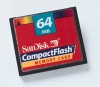
SanDisk CompactFlash Memory Card OEM Product Manual Version 12.0 Document No. 20-10-00038 02/2007 SanDisk Corporation Corporate Headquarters 601 McCarthy Boulevard Milpitas, CA 95035 (408) 801-1000 Phone (408) 801-8657 Fax www.sandisk.com
SanDisk CompactFlash Memory Card OEM Product Manual Version 12.0 Document No. 20-10-00038 02/2007 SanDisk Corporation Corporate Headquarters 601 McCarthy Boulevard Milpitas, CA 95035 (408) 801-1000 Phone (408) 801-8657 Fax www.sandisk.com
Product Manual
Page 3
..., registered in the United States and other countries. Document 20-10-00038 Rev. 12.0 Revision History Date February 2007 Revision 12.0 Description Merged CFlash 11.2 manual with CFA Spec v4.0. © 2007 SanDisk Corporation i Rev. 12.0, 02/07 SanDisk CompactFlash Card OEM Product Manual SanDisk® Corporation general policy does not recommend the use of its...
..., registered in the United States and other countries. Document 20-10-00038 Rev. 12.0 Revision History Date February 2007 Revision 12.0 Description Merged CFlash 11.2 manual with CFA Spec v4.0. © 2007 SanDisk Corporation i Rev. 12.0, 02/07 SanDisk CompactFlash Card OEM Product Manual SanDisk® Corporation general policy does not recommend the use of its...

Product Manual
Page 8
... • Minimum 10,000 insertions 1.3 Scope This document describes the key features and specifications of CompactFlash Memory cards, as well as the information required to a host system. Retail CompactFlash specifications are not covered in this product to interface this manual. 1.4 CompactFlash Standard SanDisk CompactFlash Memory cards are fully compatible with the CompactFlash Specification published by the CompactFlash Association. CompactFlash Association P.O. Box...
... • Minimum 10,000 insertions 1.3 Scope This document describes the key features and specifications of CompactFlash Memory cards, as well as the information required to a host system. Retail CompactFlash specifications are not covered in this product to interface this manual. 1.4 CompactFlash Standard SanDisk CompactFlash Memory cards are fully compatible with the CompactFlash Specification published by the CompactFlash Association. CompactFlash Association P.O. Box...

Product Manual
Page 11
..., but this to the card is accessing it, thus conserving power. SanDisk CompactFlash Card OEM Product Manual Introduction 1.7.5 Automatic Sleep Mode A unique feature of the SanDisk CompactFlash Memory Card is improved through the reduction... of overhead but it is no further commands are received within 5 msec. The delay from sleep mode. This same procedure of 3.30 volts ± 5% or 5.00 volts ± 10...
..., but this to the card is accessing it, thus conserving power. SanDisk CompactFlash Card OEM Product Manual Introduction 1.7.5 Automatic Sleep Mode A unique feature of the SanDisk CompactFlash Memory Card is improved through the reduction... of overhead but it is no further commands are received within 5 msec. The delay from sleep mode. This same procedure of 3.30 volts ± 5% or 5.00 volts ± 10...

Product Manual
Page 14
... mV max. Maximum average value. 5V +/- 10% 500 µ 800 µ 1.2 mA 55 mA 70 mA 100 mA 500 µ 800 µ 1.2 mA 100 mA 100 mA 100 mA 02/07, Rev. 12.0 2-2 © 2007 SanDisk Corporation ripple (p-p) 3.3V +/- 5% Memory Subsystema CompactFlash Memory Card Sleep Up to 512 MB 300 µ 1.0 GB 600 µ Over...
... mV max. Maximum average value. 5V +/- 10% 500 µ 800 µ 1.2 mA 55 mA 70 mA 100 mA 500 µ 800 µ 1.2 mA 100 mA 100 mA 100 mA 02/07, Rev. 12.0 2-2 © 2007 SanDisk Corporation ripple (p-p) 3.3V +/- 5% Memory Subsystema CompactFlash Memory Card Sleep Up to 512 MB 300 µ 1.0 GB 600 µ Over...
Product Manual
Page 16
Product Specifications SanDisk CompactFlash Card OEM Product Manual 2.4 System Reliability Table 2-4 Reliability MTBF (@ 25 C) Preventative Maintenance Data Reliability >1,000,000 hours None
Product Specifications SanDisk CompactFlash Card OEM Product Manual 2.4 System Reliability Table 2-4 Reliability MTBF (@ 25 C) Preventative Maintenance Data Reliability >1,000,000 hours None
Product Manual
Page 19
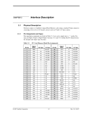
...OPEN I2Z OT1 OT1 I3U I1U,OT1 I1U,OT1 I1Z,OZ3 I1Z,OZ3 I1Z,OZ3 Ground © 2007 SanDisk Corporation 3-1 Rev. 12.0, 02/07 Table 3-1 PC Card Memory Mode Pin Assignments Pin No. 1 2 3 4 5 6 7 8 9 10 11 12 13 14 15 16 17 18 19 20 21 22 23 24 25 Signal Name GND ...VCC A06 A05 A04 A03 A02 A01 A00 D00 D01 D02 WP -CD2 Pin Type - I - CHAPTER 3 Interface Description 3.1 Physical Description The host connects to SanDisk CompactFlash Memory cards using a standard 50-pin connector consisting of two rows of 25 female contacts each on 50 mil (1.27 mm) centers. 3.1.1 Pin Assignments and Types The...
...OPEN I2Z OT1 OT1 I3U I1U,OT1 I1U,OT1 I1Z,OZ3 I1Z,OZ3 I1Z,OZ3 Ground © 2007 SanDisk Corporation 3-1 Rev. 12.0, 02/07 Table 3-1 PC Card Memory Mode Pin Assignments Pin No. 1 2 3 4 5 6 7 8 9 10 11 12 13 14 15 16 17 18 19 20 21 22 23 24 25 Signal Name GND ...VCC A06 A05 A04 A03 A02 A01 A00 D00 D01 D02 WP -CD2 Pin Type - I - CHAPTER 3 Interface Description 3.1 Physical Description The host connects to SanDisk CompactFlash Memory cards using a standard 50-pin connector consisting of two rows of 25 female contacts each on 50 mil (1.27 mm) centers. 3.1.1 Pin Assignments and Types The...
Product Manual
Page 20
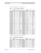
...OZ3 I1Z,OZ3 I1Z,OZ3 I3Z Ground 02/07, Rev. 12.0 3-2 © 2007 SanDisk Corporation Name Pin Type I /O - I O I O O I I/O I/O I/O I/O I /O Type Pin No. 1 GND - Interface Description SanDisk CompactFlash Card OEM Product Manual PC Card I /O Mode Pin Assignments Signal Name GND D03 D04 D05 D06 D07 -CE1 A10 ...-OE A09 A08 A07 VCC A06 A05 A04 A03 A02 A01 A00 D00 D01 D02 -IOIS16 -CD2 Pin Type - Table 3-2 Pin No. 1 2 3 4 5 6 7 8 9 10 11 12...
...OZ3 I1Z,OZ3 I1Z,OZ3 I3Z Ground 02/07, Rev. 12.0 3-2 © 2007 SanDisk Corporation Name Pin Type I /O - I O I O O I I/O I/O I/O I/O I /O Type Pin No. 1 GND - Interface Description SanDisk CompactFlash Card OEM Product Manual PC Card I /O Mode Pin Assignments Signal Name GND D03 D04 D05 D06 D07 -CE1 A10 ...-OE A09 A08 A07 VCC A06 A05 A04 A03 A02 A01 A00 D00 D01 D02 -IOIS16 -CD2 Pin Type - Table 3-2 Pin No. 1 2 3 4 5 6 7 8 9 10 11 12...
Product Manual
Page 21
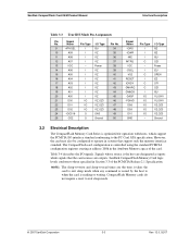
... configured to those specified in Section 3.3 of the card. SanDisk CompactFlash Memory Card logic levels conform to operate in the Attribute Memory space of the PCMCIA Release 2.1 Specification. Name Pin Type I/O Type Pin No. 9 -ATA SEL I I3U 34 10 A09 I I1Z 35 11 A08 I I1Z 36 12...WE INTRQ VCC -CSEL -VS2 RESET IORDY -DMARQ -DMACK -DASP -PDIAG D08 D09 D10 GND Pin Type I I I /O - SanDisk CompactFlash Card OEM Product Manual Interface Description Table 3-3 True IDE Mode Pin Assignments Pin Signal No. Signals whose source is controlled using the standard PCMCIA ...
... configured to those specified in Section 3.3 of the card. SanDisk CompactFlash Memory Card logic levels conform to operate in the Attribute Memory space of the PCMCIA Release 2.1 Specification. Name Pin Type I/O Type Pin No. 9 -ATA SEL I I3U 34 10 A09 I I1Z 35 11 A08 I I1Z 36 12...WE INTRQ VCC -CSEL -VS2 RESET IORDY -DMARQ -DMACK -DASP -PDIAG D08 D09 D10 GND Pin Type I I I /O - SanDisk CompactFlash Card OEM Product Manual Interface Description Table 3-3 True IDE Mode Pin Assignments Pin Signal No. Signals whose source is controlled using the standard PCMCIA ...
Product Manual
Page 22
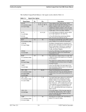
...10, 11, 12, 14, These address lines, along with this input/output is the Pass Diagnostic signal in the master/slave handshake protocol. Table 3-4 Signal Description Signal Name Dir. They are used by the host to determine if the card is fully inserted into its configuration control and status registers. Interface Description SanDisk CompactFlash Card... OEM Product Manual The SanDisk CompactFlash Memory Card signals are used both to select the card and to ...
...10, 11, 12, 14, These address lines, along with this input/output is the Pass Diagnostic signal in the master/slave handshake protocol. Table 3-4 Signal Description Signal Name Dir. They are used by the host to determine if the card is fully inserted into its configuration control and status registers. Interface Description SanDisk CompactFlash Card... OEM Product Manual The SanDisk CompactFlash Memory Card signals are used both to select the card and to ...

Product Manual
Page 26
... 3-5, "x" refers to reduce power use. 02/07, Rev. 12.0 3-8 © 2007 SanDisk Corporation Interface Description SanDisk CompactFlash Card OEM Product Manual Table 3-4 Signal Description Signal Name Dir. V* = 0.5V min. Characteristics for the... -I /O Operation, pin 24 is used for the CompactFlash Memory Card Series are defined as follows: Typical conditions unless otherwise stated: VCC = 5V +/- 10% VCC...
... 3-5, "x" refers to reduce power use. 02/07, Rev. 12.0 3-8 © 2007 SanDisk Corporation Interface Description SanDisk CompactFlash Card OEM Product Manual Table 3-4 Signal Description Signal Name Dir. V* = 0.5V min. Characteristics for the... -I /O Operation, pin 24 is used for the CompactFlash Memory Card Series are defined as follows: Typical conditions unless otherwise stated: VCC = 5V +/- 10% VCC...
Product Manual
Page 27
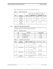
...-8 mA VCC V Vol lol= 8 mA -0.8V Gnd +0.4V X Tri-State Leakage Current loz Vol = Gnd -10 Voh = VCC 10 uA © 2007 SanDisk Corporation 3-9 Rev. 12.0, 02/07 For example-"OT3" refers to the characteristics described in Table 3-5. Table 3-6 Input ...2.0 V 0.6 0.8 1.8 2.8 V 1.0 2.0 3.3.2 Output Drive Type and Characteristics In Table 3-7 "x" refers to Totempole output with a Type 3 output drive characteristic. SanDisk CompactFlash Card OEM Product Manual Interface Description Table 3-6 defines the input characteristics of the parameters in Table 3-8.
...-8 mA VCC V Vol lol= 8 mA -0.8V Gnd +0.4V X Tri-State Leakage Current loz Vol = Gnd -10 Voh = VCC 10 uA © 2007 SanDisk Corporation 3-9 Rev. 12.0, 02/07 For example-"OT3" refers to the characteristics described in Table 3-5. Table 3-6 Input ...2.0 V 0.6 0.8 1.8 2.8 V 1.0 2.0 3.3.2 Output Drive Type and Characteristics In Table 3-7 "x" refers to Totempole output with a Type 3 output drive characteristic. SanDisk CompactFlash Card OEM Product Manual Interface Description Table 3-6 defines the input characteristics of the parameters in Table 3-8.

Product Manual
Page 28
Table 3-9 Power Up/Power Down Timing Item Value CE Signal Levela CE Setup Time CE Setup Time CE Recover Time VCC Rising Timeb VCC Falling Timeb Reset Width Symbol Vi (CE) TSU (VCC) TSU (RESET) TREC (VCC) tpr tpf TW (RESET) Th (Hi-z Reset) TS (Hi-z Reset) Condition 0V Interface Description SanDisk CompactFlash Card OEM Product Manual 3.3.3 Power Up/Power Down Timing The timing specification in Table 3-9 was defined to permit peripheral cards to perform powerup initialization.
Table 3-9 Power Up/Power Down Timing Item Value CE Signal Levela CE Setup Time CE Setup Time CE Recover Time VCC Rising Timeb VCC Falling Timeb Reset Width Symbol Vi (CE) TSU (VCC) TSU (RESET) TREC (VCC) tpr tpf TW (RESET) Th (Hi-z Reset) TS (Hi-z Reset) Condition 0V Interface Description SanDisk CompactFlash Card OEM Product Manual 3.3.3 Power Up/Power Down Timing The timing specification in Table 3-9 was defined to permit peripheral cards to perform powerup initialization.

Product Manual
Page 29
SanDisk CompactFlash Card OEM Product Manual Interface Description Figure 3-2 Power Up/Power Down Timing for all types of memory. Skews and delays from Add Changea Address Setup Time ... tGHQZ tEHQZ tELQNZ tGLQNZ tAXQX tAVGL 100 ns Min. 100 ----------- 5 5 0 10 Max. --100 100 50 50 50 --------- © 2007 SanDisk Corporation 3-11 Rev. 12.0, 02/07 Table 3-10 Common Memory Read Timing Specification Speed Version Item Read Cycle Time Address Access Timea Card Enable Access Time Output Enable Access Time Output Disable Time from...
SanDisk CompactFlash Card OEM Product Manual Interface Description Figure 3-2 Power Up/Power Down Timing for all types of memory. Skews and delays from Add Changea Address Setup Time ... tGHQZ tEHQZ tELQNZ tGLQNZ tAXQX tAVGL 100 ns Min. 100 ----------- 5 5 0 10 Max. --100 100 50 50 50 --------- © 2007 SanDisk Corporation 3-11 Rev. 12.0, 02/07 Table 3-10 Common Memory Read Timing Specification Speed Version Item Read Cycle Time Address Access Timea Card Enable Access Time Output Enable Access Time Output Disable Time from...

Product Manual
Page 30
... Enable Hold from the system driver/receiver to address signal timing. 100 ns Min. 100 60 10 70 70 40 15 15 ----- 5 5 10 10 0 15 Max 50 50 02/07, Rev. 12.0 3-12 © 2007 SanDisk Corporation Interface Description SanDisk CompactFlash Card OEM Product Manual Table 3-10 Common Memory Read Timing Specification Speed Version Item Address Hold Time...
... Enable Hold from the system driver/receiver to address signal timing. 100 ns Min. 100 60 10 70 70 40 15 15 ----- 5 5 10 10 0 15 Max 50 50 02/07, Rev. 12.0 3-12 © 2007 SanDisk Corporation Interface Description SanDisk CompactFlash Card OEM Product Manual Table 3-10 Common Memory Read Timing Specification Speed Version Item Address Hold Time...

Product Manual
Page 35
SanDisk CompactFlash Card OEM Product Manual Interface Description Table 3-14 contains the specification information related to the I /O Write Timing Specification Item Data Setup before -IOWR Data Hold following -... value that will be greater than or equal to the asserted condi tion. NOTE: SanDisk CompactFlash Memory cards do not assert an -IORDY signal. © 2007 SanDisk Corporation 3-17 Rev. 12.0, 02/07 Max. (ns 35a 35 35 35 3.3.10 True IDE Mode The following -IOWR -IOIS16 Delay falling from Address -IOIS16 Delay rising...
SanDisk CompactFlash Card OEM Product Manual Interface Description Table 3-14 contains the specification information related to the I /O Write Timing Specification Item Data Setup before -IOWR Data Hold following -... value that will be greater than or equal to the asserted condi tion. NOTE: SanDisk CompactFlash Memory cards do not assert an -IORDY signal. © 2007 SanDisk Corporation 3-17 Rev. 12.0, 02/07 Max. (ns 35a 35 35 35 3.3.10 True IDE Mode The following -IOWR -IOIS16 Delay falling from Address -IOIS16 Delay rising...

Product Manual
Page 36
...Device PIO Timing Parameters t0 a Cycle time (min.) t1 Address valid to address valid hold (min.) Mode 4 (ns) 120 25 70 25 20 10 20 5 30 10 a. setup (min.) t2 a IORD-/IOWR- data hold (min.) t6z b IORD- t0 is the minimum total cycle time, t2 is the minimum ...-CS1 and -DA(2:0). data hold (min.) t5 IORD- data setup (min.) t6 IORD- recovery time (min.) t3 IOWR- to IORD-/IOWR- Interface Description SanDisk CompactFlash Card OEM Product Manual Figure 3-7 Register Transfer to ensure that the data bus is no longer driven by the device (tri-state). 02/07, Rev. 12...
...Device PIO Timing Parameters t0 a Cycle time (min.) t1 Address valid to address valid hold (min.) Mode 4 (ns) 120 25 70 25 20 10 20 5 30 10 a. setup (min.) t2 a IORD-/IOWR- data hold (min.) t6z b IORD- t0 is the minimum total cycle time, t2 is the minimum ...-CS1 and -DA(2:0). data hold (min.) t5 IORD- data setup (min.) t6 IORD- recovery time (min.) t3 IOWR- to IORD-/IOWR- Interface Description SanDisk CompactFlash Card OEM Product Manual Figure 3-7 Register Transfer to ensure that the data bus is no longer driven by the device (tri-state). 02/07, Rev. 12...

Product Manual
Page 38
... 30 80 70 30 10 20 5 30 10 Mode 4 (ns) 120 25 70 25 20 10 20 5 30 10 a. data hold (min.) t6zb IORD- NOTE: SanDisk CompactFlash Memory cards do not assert an -IORDY signal. Interface Description SanDisk CompactFlash Card OEM Product Manual The PIO data transfer parameters are identified by the device (tri-state). 3.4 Card Configuration SanDisk CompactFlash Memory cards are defined in...
... 30 80 70 30 10 20 5 30 10 Mode 4 (ns) 120 25 70 25 20 10 20 5 30 10 a. data hold (min.) t6zb IORD- NOTE: SanDisk CompactFlash Memory cards do not assert an -IORDY signal. Interface Description SanDisk CompactFlash Card OEM Product Manual The PIO data transfer parameters are identified by the device (tri-state). 3.4 Card Configuration SanDisk CompactFlash Memory cards are defined in...

Product Manual
Page 51
... locked out from the host through the Data Register. The bits in some type of performing card operations. SanDisk CompactFlash Card OEM Product Manual ATA Register Set and Protocol 4.5.9 Status & Alternate Status Registers (Address-1F7[177]&3F6[376]; The meaning of the status ...device is ready. D0 ERR Set when the previous command has ended in the Error Register contain additional information describing the error. 4.5.10 Device Control Register (Address-3F6[376]; Reading the Status Register clears a pending interrupt while reading the Auxiliary Status Register does not.
... locked out from the host through the Data Register. The bits in some type of performing card operations. SanDisk CompactFlash Card OEM Product Manual ATA Register Set and Protocol 4.5.9 Status & Alternate Status Registers (Address-1F7[177]&3F6[376]; The meaning of the status ...device is ready. D0 ERR Set when the previous command has ended in the Error Register contain additional information describing the error. 4.5.10 Device Control Register (Address-3F6[376]; Reading the Status Register clears a pending interrupt while reading the Auxiliary Status Register does not.
Product Manual
Page 54
ATA Register Set and Protocol SanDisk CompactFlash Card OEM Product Manual -This page intentionally left blank- 02/07, Rev. 12.0 4-10 © 2007 SanDisk Corporation
ATA Register Set and Protocol SanDisk CompactFlash Card OEM Product Manual -This page intentionally left blank- 02/07, Rev. 12.0 4-10 © 2007 SanDisk Corporation