Product Manual
Page 19
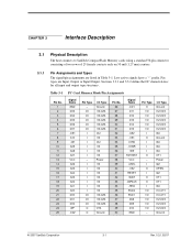
... for all input and output type structures.. Table 3-1 PC Card Memory Mode Pin Assignments Pin No. 1 2 3 4 5 6 7 8 9 10 11 12 13 14 15 16 17 18 19 20 21 22 23 24 25 Signal Name GND D03 D04 D05 D06 D07 -CE1 A10 -OE A09 A08 A07 VCC A06 A05 A04 A03 A02... OPEN I2Z OT1 OT1 I3U I1U,OT1 I1U,OT1 I1Z,OZ3 I1Z,OZ3 I1Z,OZ3 Ground © 2007 SanDisk Corporation 3-1 Rev. 12.0, 02/07 CHAPTER 3 Interface Description 3.1 Physical Description The host connects to SanDisk CompactFlash Memory cards using a standard 50-pin connector consisting of two rows of 25 female contacts each on 50 mil...
... for all input and output type structures.. Table 3-1 PC Card Memory Mode Pin Assignments Pin No. 1 2 3 4 5 6 7 8 9 10 11 12 13 14 15 16 17 18 19 20 21 22 23 24 25 Signal Name GND D03 D04 D05 D06 D07 -CE1 A10 -OE A09 A08 A07 VCC A06 A05 A04 A03 A02... OPEN I2Z OT1 OT1 I3U I1U,OT1 I1U,OT1 I1Z,OZ3 I1Z,OZ3 I1Z,OZ3 Ground © 2007 SanDisk Corporation 3-1 Rev. 12.0, 02/07 CHAPTER 3 Interface Description 3.1 Physical Description The host connects to SanDisk CompactFlash Memory cards using a standard 50-pin connector consisting of two rows of 25 female contacts each on 50 mil...
Product Manual
Page 20
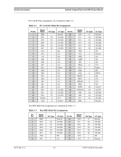
...OZ3 29 5 D06 I/O I1Z,OZ3 30 6 D07 I/O I1Z,OZ3 31 7 -CS0 I I3Z 32 8 A10 I I1Z 33 Signal Name -CD1 D11 D12 D13 D14 D15 -CS1 -VS1 Pin Type O I/O I/O I/O I/O I/O I O I O - Interface Description SanDisk CompactFlash Card OEM Product Manual PC Card I/O Pin Assignments are contained in Table 3-2. I O I O O I I/O I/O I/O I/O I /O ... No. Name Pin Type I /O - I/O I/O I/O I/O I/O I I I I I I /O Mode Pin Assignments Signal Name GND D03 D04 D05 D06 D07 -CE1 A10 -OE A09 A08 A07 VCC A06 A05 A04 A03 A02 A01 A00 D00 D01 D02 -IOIS16 -CD2 Pin Type - Table 3-2 Pin No. 1 2 3 4 5 6...
...OZ3 29 5 D06 I/O I1Z,OZ3 30 6 D07 I/O I1Z,OZ3 31 7 -CS0 I I3Z 32 8 A10 I I1Z 33 Signal Name -CD1 D11 D12 D13 D14 D15 -CS1 -VS1 Pin Type O I/O I/O I/O I/O I/O I O I O - Interface Description SanDisk CompactFlash Card OEM Product Manual PC Card I/O Pin Assignments are contained in Table 3-2. I O I O O I I/O I/O I/O I/O I /O ... No. Name Pin Type I /O - I/O I/O I/O I/O I/O I I I I I I /O Mode Pin Assignments Signal Name GND D03 D04 D05 D06 D07 -CE1 A10 -OE A09 A08 A07 VCC A06 A05 A04 A03 A02 A01 A00 D00 D01 D02 -IOIS16 -CD2 Pin Type - Table 3-2 Pin No. 1 2 3 4 5 6...
Product Manual
Page 22
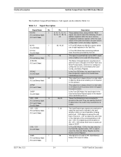
... -CE1 accesses the even byte or the Odd byte of eight registers in the Task File. Interface Description SanDisk CompactFlash Card OEM Product Manual The SanDisk CompactFlash Memory Card signals are described in the master/slave handshake protocol. A2-A0 (True IDE Mode) I 18, 19,... 20 In True IDE Mode only A[2:0] is used to changes in Memory Mode since a battery is fully inserted into its configuration control and status registers. Pin Description A10...
... -CE1 accesses the even byte or the Odd byte of eight registers in the Task File. Interface Description SanDisk CompactFlash Card OEM Product Manual The SanDisk CompactFlash Memory Card signals are described in the master/slave handshake protocol. A2-A0 (True IDE Mode) I 18, 19,... 20 In True IDE Mode only A[2:0] is used to changes in Memory Mode since a battery is fully inserted into its configuration control and status registers. Pin Description A10...
Product Manual
Page 39
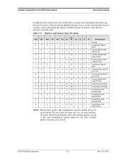
... memory except to replace status information that appears on dedicated pins in memory cards that may vary in I/O cards. Table 3-17 Registers and Memory Space Decoding A8-CE2 -CE1 -REG -OE -WE A10 A9 A4 A3 A2 A1 A0 Selected Space 1 1 X X X X X XX X X X X Standby X 0 0 0 1 X 1 XX X X X 0 Configuration Registers Read ...the CIS since these registers provide a method for accessing status information about the card that have alternate use in future products. SanDisk CompactFlash Card OEM Product Manual Interface Description In addition, these locations may be used to ...
... memory except to replace status information that appears on dedicated pins in memory cards that may vary in I/O cards. Table 3-17 Registers and Memory Space Decoding A8-CE2 -CE1 -REG -OE -WE A10 A9 A4 A3 A2 A1 A0 Selected Space 1 1 X X X X X XX X X X X Standby X 0 0 0 1 X 1 XX X X X 0 Configuration Registers Read ...the CIS since these registers provide a method for accessing status information about the card that have alternate use in future products. SanDisk CompactFlash Card OEM Product Manual Interface Description In addition, these locations may be used to ...
Product Manual
Page 40
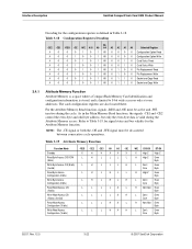
... Valid Even Byte Write Word Access Configuration (16 bits) L L L H X H L Don't Even Care Byte 02/07, Rev. 12.0 3-22 © 2007 SanDisk Corporation The card configuration registers are also located there. Interface Description SanDisk CompactFlash Card OEM Product Manual Decoding for the configuration registers is defined in the Main Memory Read functions, the signals -CE1 and...
... Valid Even Byte Write Word Access Configuration (16 bits) L L L H X H L Don't Even Care Byte 02/07, Rev. 12.0 3-22 © 2007 SanDisk Corporation The card configuration registers are also located there. Interface Description SanDisk CompactFlash Card OEM Product Manual Decoding for the configuration registers is defined in the Main Memory Read functions, the signals -CE1 and...

Product Manual
Page 47
...random access to even addresses between 400h and 7FFh access register 9. SanDisk CompactFlash Card OEM Product Manual ATA Register Set and Protocol 4.3 Memory Mapped Addressing When CompactFlash Memory Card registers are byte accessed in the order 9 then 8 the data...; vided so that lie at offset 0 and 1. Repeated byte accesses to odd addresses between 400h and 7FFh access register 8. Table 4-4 Memory Mapped Decoding A9-REG A10 A4 A3 A2 A1 A0 Offset -OE=0 -WE=0 1 0 X 0 0 0 0 0 Even RD Dataa Even WR Dataa 1 0 X 0 0 0 1 1 Error Registerb Featuresb 1 0 X 0 0...
...random access to even addresses between 400h and 7FFh access register 9. SanDisk CompactFlash Card OEM Product Manual ATA Register Set and Protocol 4.3 Memory Mapped Addressing When CompactFlash Memory Card registers are byte accessed in the order 9 then 8 the data...; vided so that lie at offset 0 and 1. Repeated byte accesses to odd addresses between 400h and 7FFh access register 8. Table 4-4 Memory Mapped Decoding A9-REG A10 A4 A3 A2 A1 A0 Offset -OE=0 -WE=0 1 0 X 0 0 0 0 0 Even RD Dataa Even WR Dataa 1 0 X 0 0 0 1 1 Error Registerb Featuresb 1 0 X 0 0...
